Semiconductor device manufacturing method

a manufacturing method and semiconductor technology, applied in the direction of semiconductor devices, electrical devices, transistors, etc., can solve the problems of reducing productivity, reducing resistance, and reducing the blocking voltage of the reverse, so as to increase the electron mobility, reduce the thermal diffusion time, and increase the performance of the igbt

Active Publication Date: 2011-11-17
FUJI ELECTRIC CO LTD
View PDF2 Cites 10 Cited by
  • Summary
  • Abstract
  • Description
  • Claims
  • Application Information

AI Technical Summary

Benefits of technology

[0040]According to the invention, by connecting the thermal diffusion layer formed from the front surface and the in-groove diffusion layer formed from the back surface, thus forming the separation layer, it is possible to form the thermal diffusion layer shallowly, and it is possible to considerably reduce the thermal diffusion time.
[0041]Also, by carrying out the ion implantation forming the in-groove diffusion layer and the ion implantation forming the collector layer separately, it is possible to select an optimum value for the tradeoff between the turn-on voltage and switching loss, while ensuring the reverse blocking voltage.
[0042]Also, by selecting <100> directions for the dicing lines, and arranging in such a way that the peripheral ends of the chips face in the <100> directions, it is possible to make the trench side wall surfaces configuring the trench gate the (100) plane, which has few interface states. By forming a channel in the (100) plane, it is possible to increase the electron mobility. As a result of this, it is possible to increase the performance of the IGBT.
[0043]Also, by making the direction of the grooves formed from the back surface of the wafer a <100> direction, they intersect with the cleavage direction at 45°. For this reason, a cleavage is unlikely to occur, and it is possible to increase the mechanical strength of the wafer. As a result of this, it is possible to reduce wafer breakage and chipping when handling in-process, and it is possible to improve the yield rate.

Problems solved by technology

The oxygen becomes a donor, reducing the resistance, and causing a disadvantage such as a reduction in the blocking voltage of the reverse blocking IGBT.
Also, as a long time in the region of 300 hours (approximately two weeks) is necessary for one thermal process, throughput is extremely poor, leading to a reduction in productivity.
For example, when the impurity concentration of the groove diffusion layer is optimized, the tradeoff between the turn-on voltage and switching loss deteriorates.
Also, when the impurity concentration of the p-collector layer is optimized, it is difficult to ensure the blocking voltage.
Also, as the grooves are formed from the back side to near the front surface, the mechanical strength of the wafer is low, and it may break when handling.
In JP-A-2005-93972 (FIG. 2), as deep grooves are formed from the front surface side reaching the p-collector layer on the back surface side, the mechanical strength of the wafer is low, and it may break when handling.
In JP-A-2004-336008 (FIG. 1), as the dicing line is on the outer side of the separation layer, the chips increase in size, and the chip cost increases.
In JP-A-2009-177039 (FIG. 7), as the chips are stacked after dicing and an ion implantation is carried out into a side surface thereof, it may happen that the surfaces of the chips are scratched, leading to a reduction in device performance.

Method used


Image

  • Semiconductor device manufacturing method
  • Semiconductor device manufacturing method
  • Semiconductor device manufacturing method

Examples


working example 1

[0065]FIGS. 1A to 4J, showing a semiconductor device manufacturing method of a first working example of the invention, are main portion manufacturing step sectional views shown in order of step. This is an example of a reverse blocking IGBT having a planar gate structure.

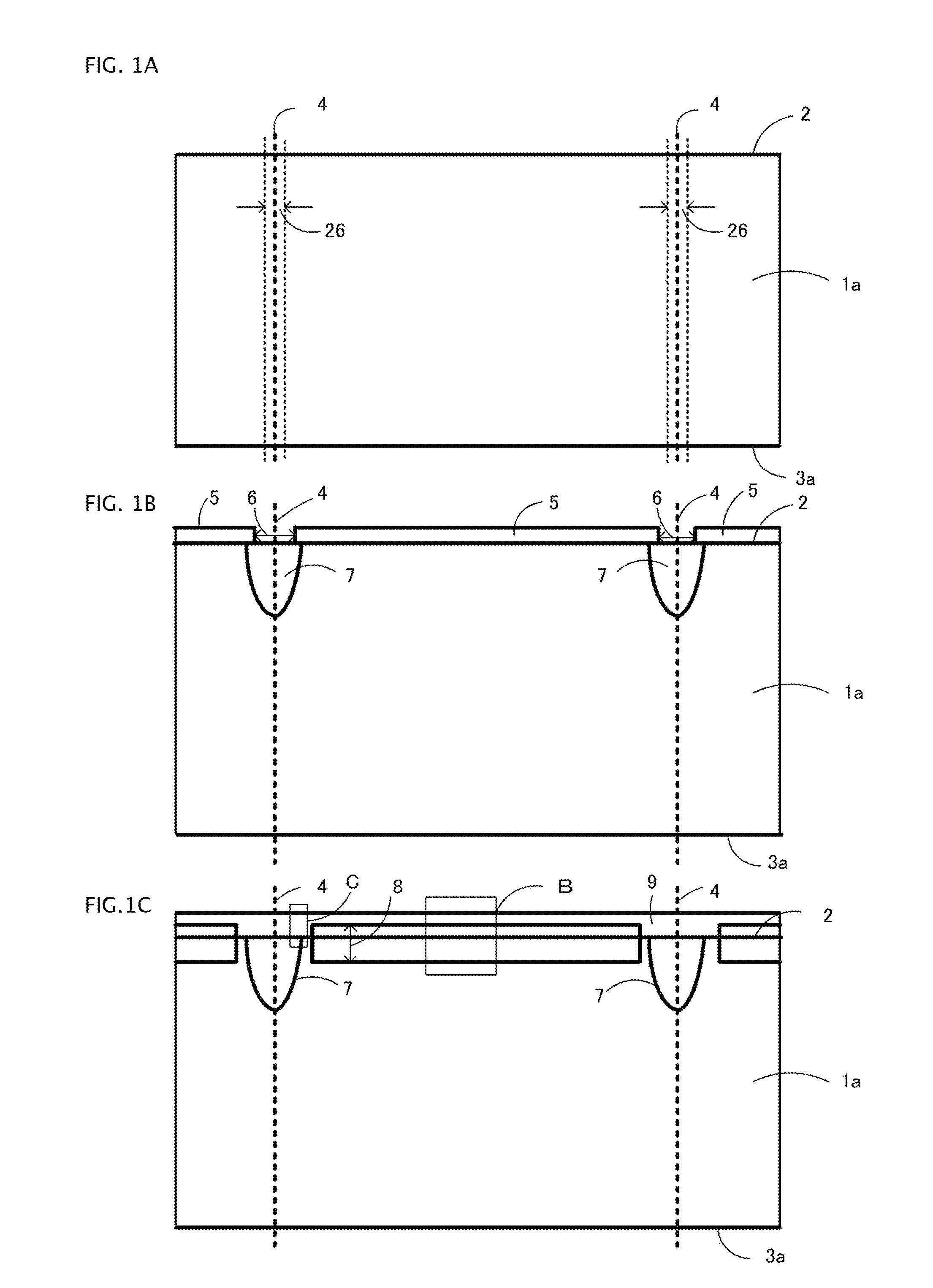
[0066]Firstly, in FIG. 1A, wafer 1a with a thickness in the region of, for example, 400 μm, wherein the directions of orientation flat (OF) 25 in the (100) plane are directions, is prepared, as shown in FIGS. 5A to 5C. As the directions of OF 25 coincide with the directions of dicing lines 26 when chips are removed from wafer 1a, the directions of dicing lines 26 are also the directions.

[0067]FIG. 5A is a plan view of the wafer of FIG. 1A, FIG. 5B is a sectional view of FIG. 5A, and FIG. 5C is an enlarged view of an A portion of FIG. 5B. Also, the series of step sectional views are sectional views corresponding to FIG. 5C.

[0068]Next, in FIG. 1B, using mask 5 on which is formed a pattern having apertures 6 in place...

working example 2

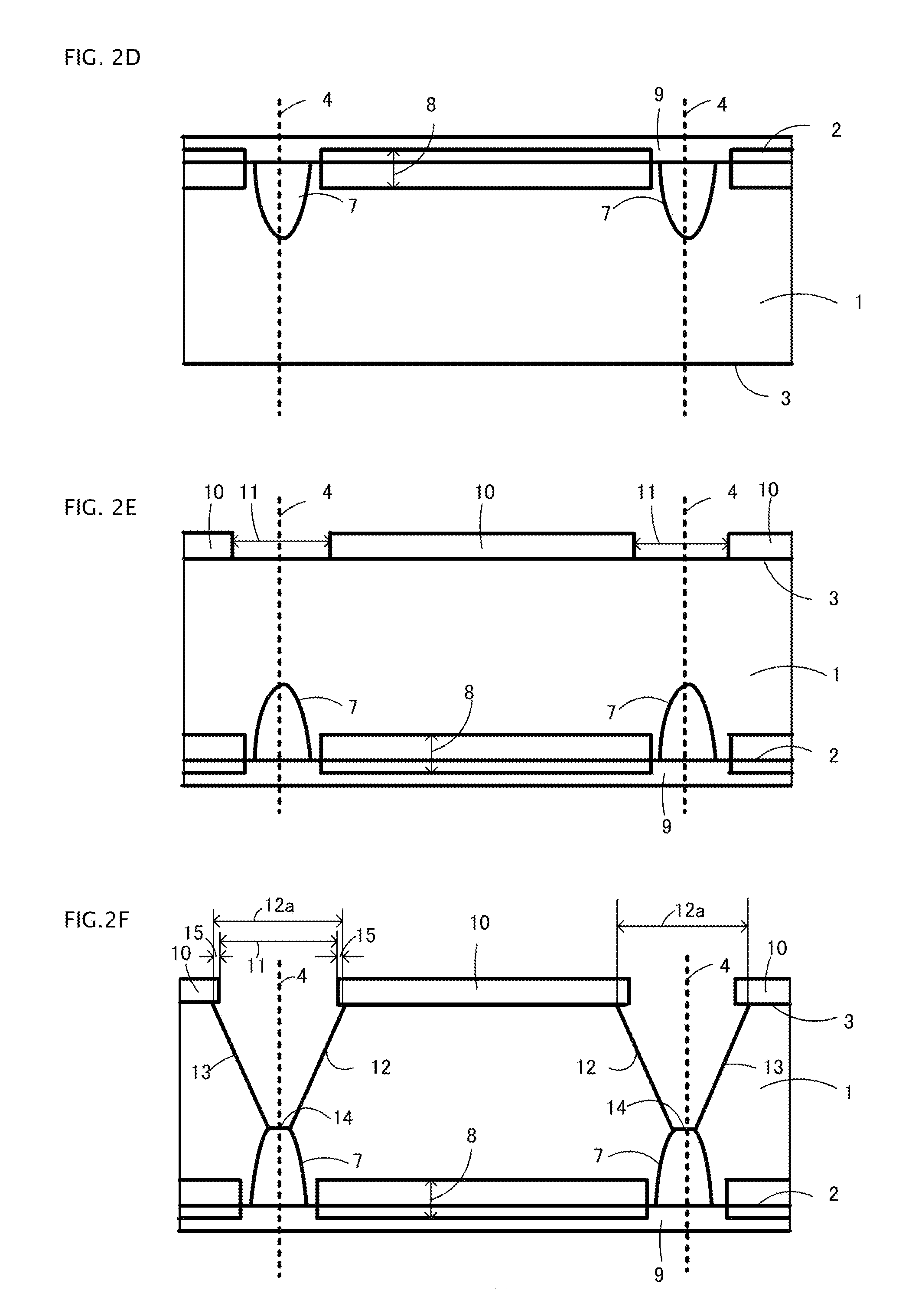
[0084]FIGS. 9A to 9C, showing a semiconductor device manufacturing method of a second working example of the invention, are main portion manufacturing step sectional views shown in order of step. A description will be given of points differing from Working Example 1. From FIG. 1A to FIG. 2D, manufacturing is carried out in the same steps as in Working Example 1.

[0085]In FIG. 9A, after the step of FIG. 2D, ion implantation 18 is carried out with an accelerating voltage of 80 keV and a dose of 1×1014 cm−2 in order to form collector layer 22. Ion implantation 18 is carried out at a tilt angle of 7° with respect to back surface 3. As conditions for ion implantation 18, it is preferable that it is carried out over the whole of back surface 3 with ranges of boron 19 of 40 keV to 150 keV for the accelerating voltage and 1×1013 cm−2 to 1×1015 cm−2 for the dose.

[0086]Next, in FIG. 9B, a resist is applied over the whole of the back surface 3. Continuing, using a double-sided exposure device, ...

working example 3

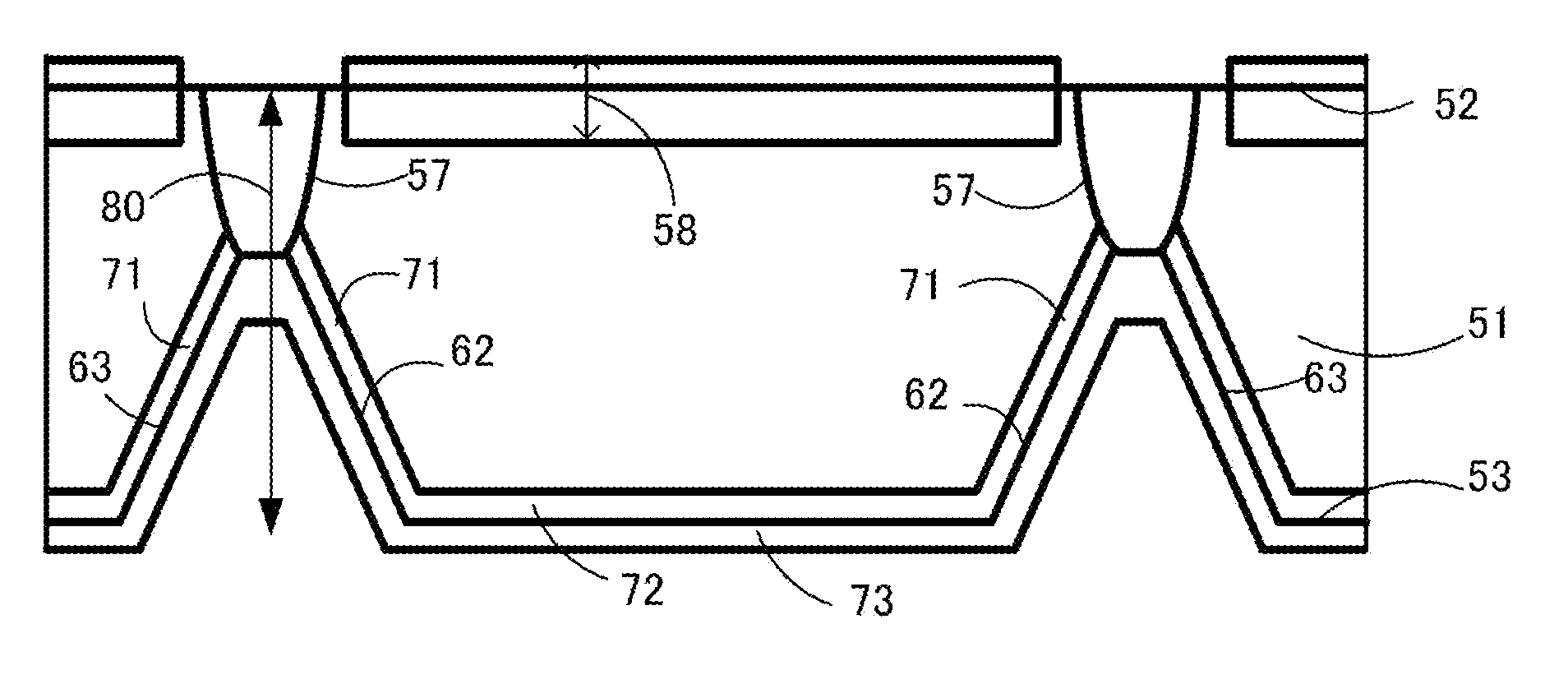
[0091]FIGS. 10A to 13J, showing a semiconductor device manufacturing method of a third working example of the invention, are main portion manufacturing step sectional views shown in order of step. This is an example of a reverse blocking IGBT having a trench gate structure.

[0092]In FIG. 10A, wafer 51a with a thickness in the region of, for example, 400 μm, wherein the directions of OF 75 in the (100) plane are directions, is prepared, as shown in FIGS. 14A to 14C. This crystal orientation is selected in order that, when making the gate structure of the IGBT a trench gate, it is possible to form the longitudinal direction of the trench perpendicular to or parallel to the directions of OF 75. By selecting these directions (orientation), it is possible to make the plane in which a channel is formed the (100) plane, which has few interface states. With the (100) plane, it is possible to increase the electron mobility, and it is possible to reduce the channel resistance. Also, as the di...


PUM

PropertyMeasurementUnit
blocking voltageaaaaaaaaaa
thicknessaaaaaaaaaa
temperatureaaaaaaaaaa

Abstract

A manufacturing method is disclosed which ensures strength of a wafer and improves device performance. A thermal diffusion layer is formed from a front surface of a wafer. A tapered groove which reaches the thermal diffusion layer is formed from a back surface by anisotropic etching with alkaline solution. In-groove thermal diffusion layer is formed on side wall surfaces of the groove. A separation layer of a reverse blocking IGBT is configured of the thermal diffusion layer and the in-groove diffusion layer. The thermal diffusion layer is formed shallowly by forming the in-groove diffusion layer. It is possible to considerably reduce thermal diffusion time. By carrying out an ion implantation forming the in-groove diffusion layer and an ion implantation forming a collector layer separately, it is possible to select an optimum value for tradeoff between turn-on voltage and switching loss, while ensuring reverse blocking voltage of the reverse blocking IGBT.

Description

BACKGROUND OF THE INVENTION[0001]A. Field of the Invention[0002]The present invention relates to a manufacturing method of a semiconductor device such as a reverse blocking IGBT (IGBT: insulated gate bipolar transistor). In particular, the invention relates to a manufacturing method whereby a separation layer of a reverse blocking IGBT is formed.[0003]B. Description of the Related Art[0004]FIGS. 18A to 18C, showing a heretofore known reverse blocking IGBT manufacturing method, are main portion manufacturing step sectional views shown in order of step. Herein, a reverse blocking IGBT with a blocking voltage of 1,200V is given as an example.[0005]In FIG. 18A, front surface 92 of silicon wafer 91a (hereafter called simply “the wafer 91a”) with a thickness in the region of 400 μm is covered with mask 95 having apertures 96. Continuing, an impurity source (for example, a boron source) is applied to mask 95, and a long-time diffusion in the region of 300 hours is carried out at a high tem...

Claims


Application Information

Patent Timeline
Patent Type & Authority Applications(United States)
IPC IPC(8): H01L21/331
CPCH01L29/045H01L29/66333H01L29/0657
Inventor OGINO, MASAAKIWAKIMOTO, HIROKIMIYAZAKI, MASAYUKI
Owner FUJI ELECTRIC CO LTD
Why Eureka
Try Eureka