Three-dimensional hot spot localization

a hot spot and three-dimensional technology, applied in the field of three-dimensional hot spot localization, can solve the problems of increasing challenges in failure analysis of modern complex systems in package devices with a three-dimensional architecture, limited access to and analysis of internal electronic structures or interconnects, and both methods are limited in resolution, so as to and improve depth resolution and measurement reliability.

Active Publication Date: 2011-12-08
DCG SYST +1
View PDF9 Cites 33 Cited by
  • Summary
  • Abstract
  • Description
  • Claims
  • Application Information

AI Technical Summary

Benefits of technology

[0016]While embodiments of the invention are described herein with respect to encapsulated integrated circuits, the invention can also be implemented for testing other devices that generate hot spots by electrical stimulation, such as batteries, solar cells, power devices, LED's, etc. Therefore, the term DUT may be applicable to these devices as well. According to embodiments of the invention, a method is provided for detecting the location of heat sources buried within a sample by using Lock-in Thermography, comprising: placing the sample on a test system; applying test signals to the sample at multiple different lock-in frequencies; while the test signals are applied to the sample, imaging the sample using an infrared sensor; detecting from the imaging lateral temperature distribution on a surface of the sample; detecting and analyzing a resulting phase shift between the test signals and thermal response obtained from the imaging in correlation to thermal heat propagation within the sample; analyzing the lateral temperature distribution to thereby obtain lateral location of the heat sources; and, analyzing the phase shift at each heat source position to thereby determine its depth location within the sample. According to embodiment of the invention, the method further comprises plotting the phase shift at various lock-in frequencies and analyzing the slope of the plotted phase vs. frequency curve in addition to the quantitative phase values to improve depth resolution and measurement reliability. The analysis may include calculating depth related phase shift to frequency behavior by analytical solution of the thermal wave propagation; and, corre...

Problems solved by technology

Failure analysis of modern complex system in package devices with a three-dimensional architecture is an increasing challenge.
The access to and analysis of internal electronic structures or interconnects is limited to non destructive techniques, like magnetic microscopy, time domain reflectometry which can be used for signal tracking.
Both methods are limited in resolution and the three dimensional positioning of electrical defects are very limited or extensive.
Standard failure localization methods like OBIRCH or Emission Microscopy can mostly not be applied ...

Method used


Image

  • Three-dimensional hot spot localization
  • Three-dimensional hot spot localization
  • Three-dimensional hot spot localization

Examples


example i

Hot Spot Depth Determination at Single Chip Devices

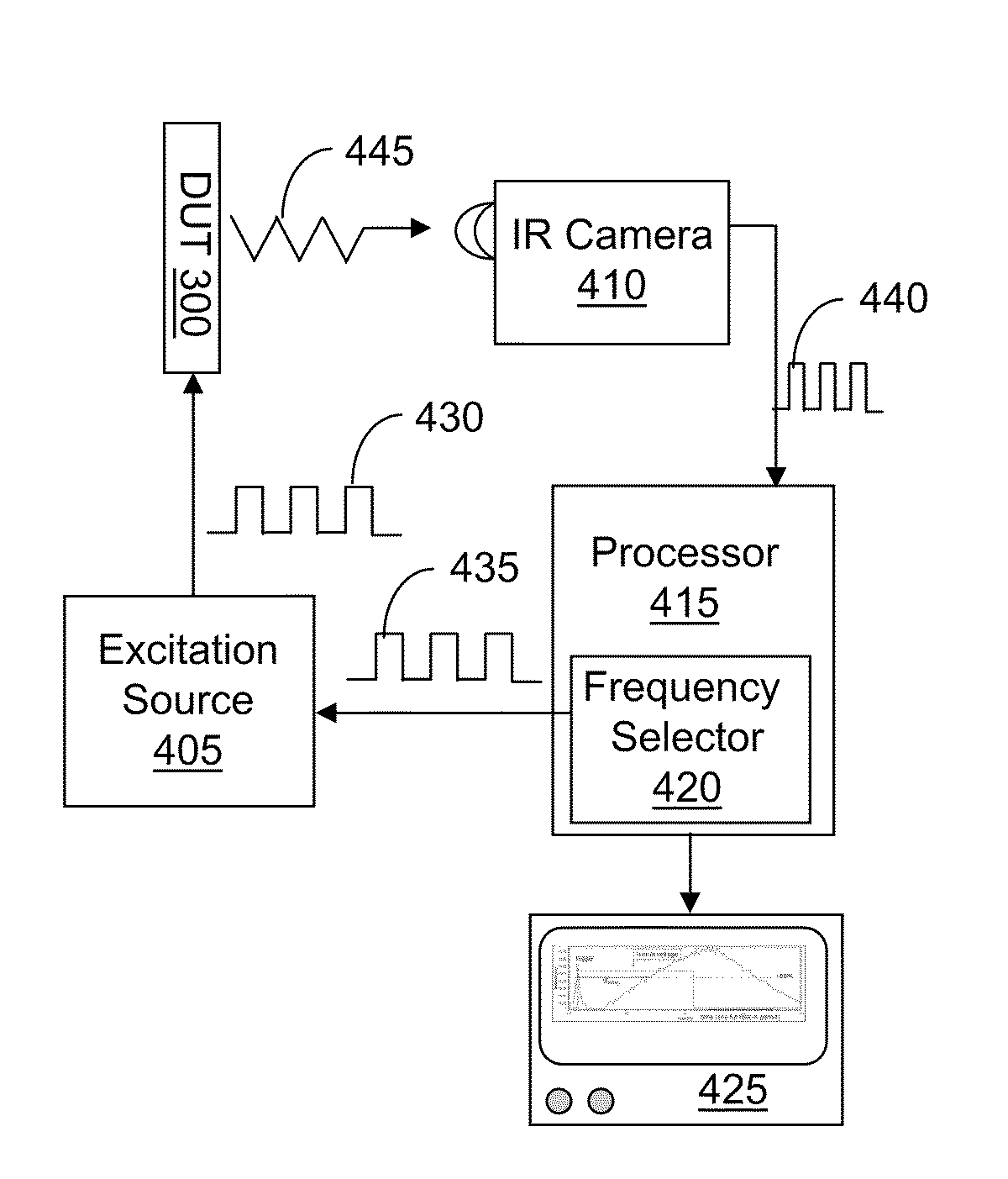
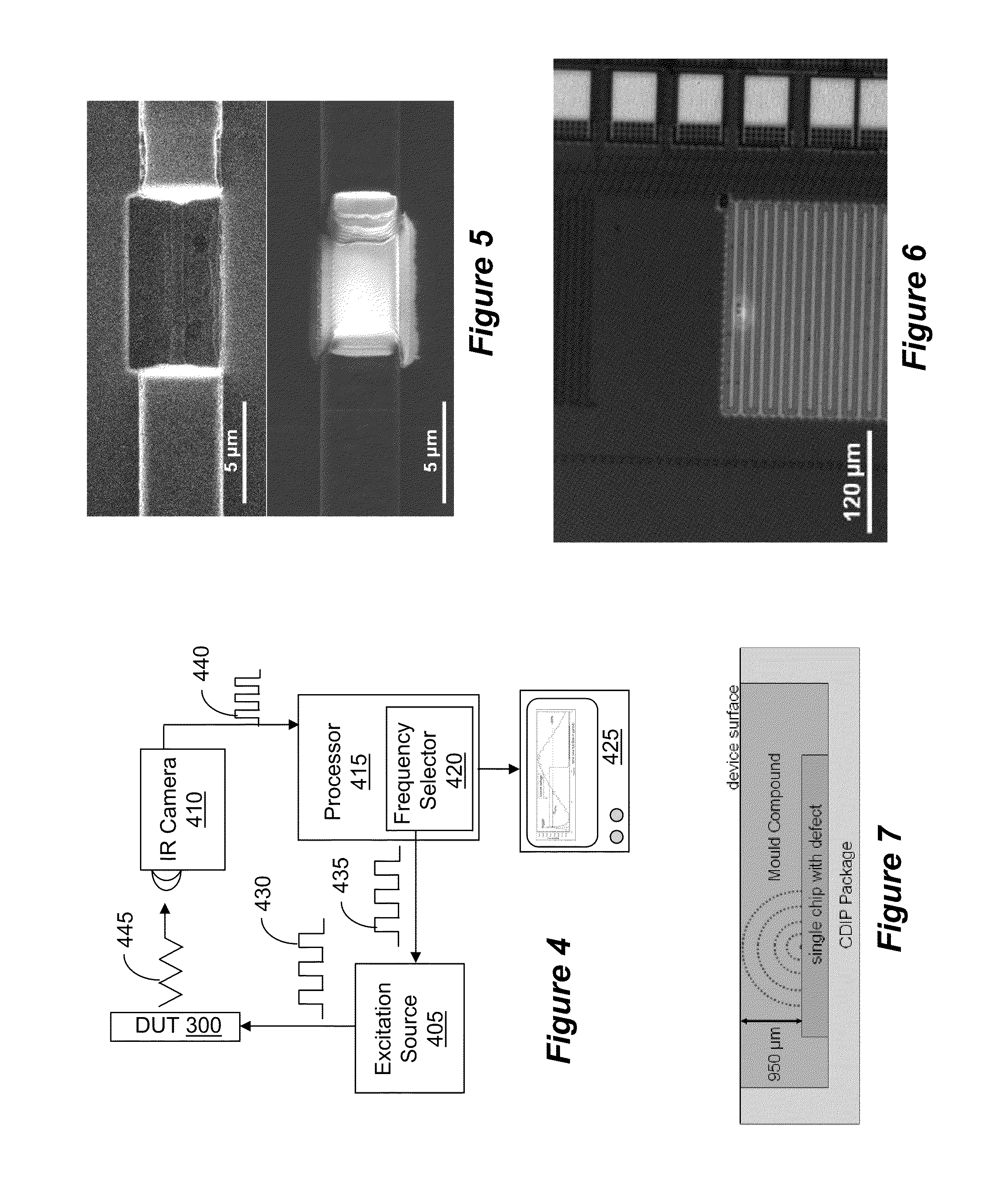
[0054]The method of LIT can be used to non-destructively determine the hot spot position inside of a fully packaged single chip device providing a better alignment for the following physical failure analysis steps. The relationship between hot spot depth, applied lock-in frequency and resulting phase shift was investigated using test structures with defined point heat sources. The test structures were made using single chip device containing a meander of copper lines. The meander was locally modified by Focused Ion Beam technique (FIB), as shown in the upper part of FIG. 5 to generate well-defined local heat sources. After the creation of the local high resistance area the single chip device was measured by LIT with a supply voltage of 1.2 V and a lock-in frequency of 5 Hz creating a local heat source with a dissipation power of 14 mW. The resulting amplitude overlaid with the topography image is shown in FIG. 6. As a next step, the...

example ii

Defect Depth Determination at Stacked Die Devices

[0060]For 3D hot spot localization inside of stacked die integrated devices, e.g., a system-in-package, a second factor of influence has to be regarded. Thermal waves generated at the hot spot position have to propagate through different material layers, e.g., silicon, mould compound, die attach tape, etc., each having different thicknesses. As a consequence, depending on the axial hot spot position at different dies of the defective device, not only the distance to the device surface but also the thermal diffusion length is changing. Therefore, thermal waves generated at hot spots at lower dies inside of the stack have to pass additional material layers compared to thermal waves generated at hot spots which are close to the device surface. Like in the previous section regarding single chip devices, this behavior can be used for the determination of the hot spot depth by calculating the theoretical phase shift over a certain frequency...

example iii

Time-Resolved Thermal Response

[0066]One disadvantage of traditional phase vs. frequency method is the long analysis time required. Measuring the phase across a full DUT with sufficient SNR may take several minutes (up to hours for high lock-in frequencies at thick, low-power samples). FIGS. 11A & 11B show a typical lock-in results, measured at flock-in=1 Hz and Vlock-in=1.2V with time of acquisition=15 minutes, with 11A being the amplitude result / image as an overlay on top of a topography image which is the basis for the localization of such a defect in x & y. FIG. 11B is the phase results, representing the local thermal delay per pixel. Since the x,y localization of a heat-source can be obtained from 11A, the final 3D analysis is reduced to the determination of the z-depth of the heat-source which only requires the phase value, measured right on top of the targeted heat-source. Therefore, taking measurement of the entire field of view, as shown in FIG. 11B for all required lock-in ...


PUM


Abstract

A non-destructive approach for the 3D localization of buried hot spots in electronic device architectures by use of Lock-in Thermography (LIT). The 3D analysis is based on the principles of thermal wave propagation through different material layers and the resulting phase shift/thermal time delay. With more complex multi level stacked die architectures it is necessary to acquire multiple LIT results at different excitation frequencies for precise hot spot depth localization. Additionally, the use of multiple time-resolved thermal waveforms, measured in a minimized field of view on top of the hot spot location, can be used to speed up the data acquisition. The shape of the resulting waveforms can be analyzed to further increase the detection accuracy and confidence level.

Description

RELATED APPLICATIONS[0001]This application claims priority benefit from U.S. Provisional Application Ser. No. 61 / 352,738, filed on Jun. 8, 2010, the entire disclosure of which is incorporated herein by reference.BACKGROUND[0002]1. Field of Invention[0003]This invention is in the field of localization of resistive heat sources (hot spots), buried inside of electronic devices. Using the described invention, the positions of hot spots can be located and pinpointed in all three dimensions by analyzing the thermal heat propagation through defect-covering layers utilizing lock in amplified thermal imaging. The invention in particular enables a non destructive 3D localization of thermal active structures or defects in a vertical stack of integrated circuits and interconnect layers within system in package devices (SiP).[0004]2. Related Art[0005]Failure analysis of modern complex system in package devices with a three-dimensional architecture is an increasing challenge. In such devices, sev...

Claims


Application Information

Patent Timeline
IPC IPC(8): G01J5/10G01J5/02
CPCG01N1/00G01N21/35G01N25/00G01R31/311G01N2021/8461G01J2005/0077G01J2005/0085G01N21/88G01J5/0066G01N25/72G01J5/485
Inventor ALTMANN, FRANKSCHMIDT, CHRISTIANSCHLANGEN, RUDOLFDESLANDES, HERVE
Owner DCG SYST
Why Eureka
Try Eureka