Dc/dc converter, power supply circuit, and semiconductor device

a technology of dc/dc converter and power supply circuit, which is applied in the direction of electric variable regulation, process and machine control, instruments, etc., can solve the problems of long continuous use time of portable electronic devices including semiconductor devices, low power consumption of semiconductor devices, etc., and achieve the improvement of power conversion efficiency, power conversion efficiency of dc-dc converter, and the effect of lowering the on-state resistance of transistors

Active Publication Date: 2011-12-15
SEMICON ENERGY LAB CO LTD
View PDF10 Cites 49 Cited by
  • Summary
  • Abstract
  • Description
  • Claims
  • Application Information

AI Technical Summary

Benefits of technology

[0017]In an embodiment of the present invention, with the aforementioned structure, the on-state resistance of a transistor is lowered in the case of high output power and the off-state current of the transistor is lowered in the case of low output power. Accordingly, anticipation of a countermeasure against the power loss taking into account the fact that a main factor of power loss depends on the magnitude of the output power allows the improvement in the power conversion efficiency of a DC-DC converter and a power supply circuit including the DC-DC converter. In addition, the power conversion efficiency of the DC-DC converter can be improved, so that power consumption of a semiconductor device including the DC-DC converter can be reduced.

Problems solved by technology

Improvement of power conversion efficiency of the DC-DC converter leads to lower power consumption of a semiconductor device and a long continuous use time of a portable electronic device including the semiconductor device.

Method used


Image

  • Dc/dc converter, power supply circuit, and semiconductor device
  • Dc/dc converter, power supply circuit, and semiconductor device
  • Dc/dc converter, power supply circuit, and semiconductor device

Examples


embodiment 1

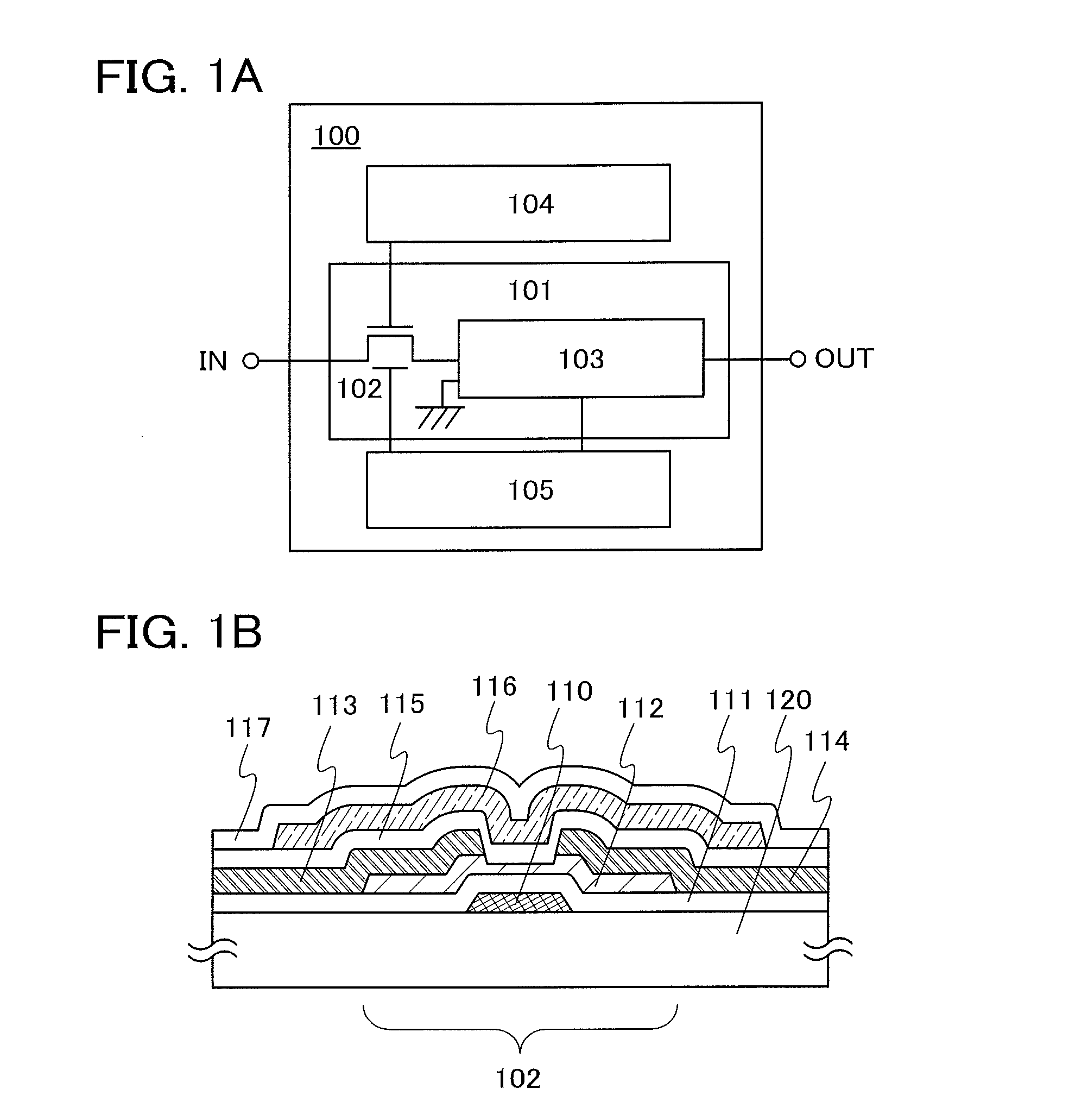
[0041]FIG. 1A illustrates an example of a structure of a DC-DC converter according to an embodiment of the present invention.

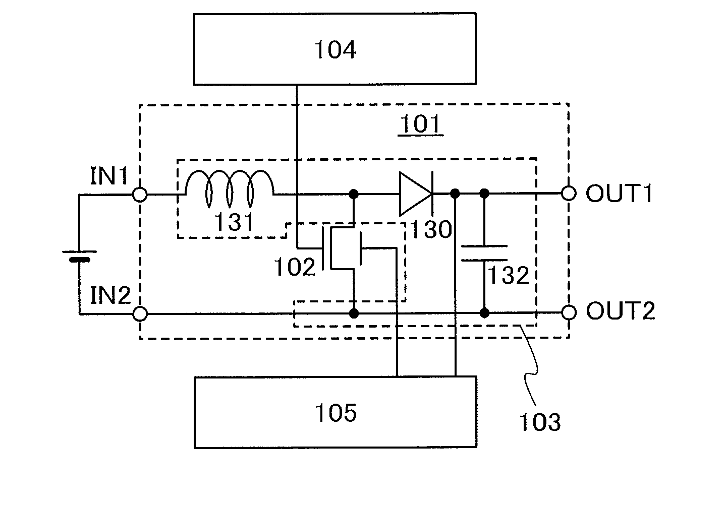
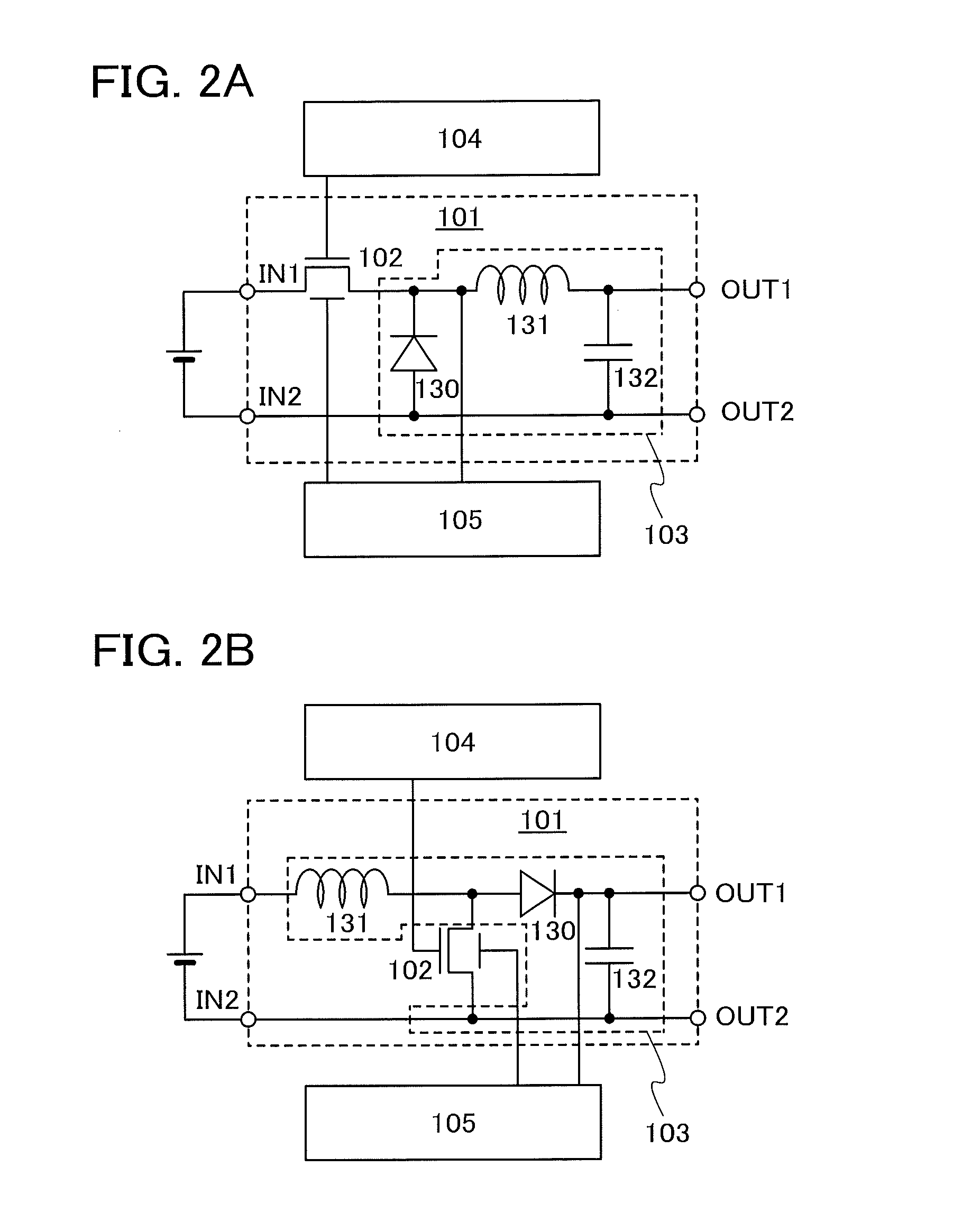
[0042]A DC-DC converter 100 illustrated in FIG. 1A includes a power conversion circuit 101 which generates a constant voltage (output voltage) by the use of voltage applied to an input terminal IN (input voltage) and outputs the constant voltage from an output terminal OUT. The power conversion circuit 101 includes a constant-voltage generation portion 103 and a transistor 102 functioning as a switching element.

[0043]When the transistor 102 is on, the input voltage is supplied to the constant-voltage generation portion 103. When the transistor 102 is off, the input voltage is not supplied to the constant-voltage generation portion 103. When the transistor 102 is turned off, a fixed voltage such as a ground potential is supplied to the constant-voltage generation portion 103. Therefore, in response to switching of the transistor 102, a pulsed signal in which th...

embodiment 2

[0093]In this embodiment, a structure and characteristics of a transistor included in the DC-DC converter of this embodiment of the present invention, and the measurement of the power conversion efficiency of the DC-DC converter including the transistor will be described.

[0094]FIG. 5A is an example of a top view of a transistor included in the DC-DC converter according to an embodiment of the present invention. FIG. 5B illustrates a cross-sectional view taken along dashed line A1-A2 in the top view of FIG. 5A.

[0095]A transistor in FIGS. 5A and 5B includes the following over a glass substrate 500: an insulating film 501, a back gate electrode 502 which is over the insulating film 501, an insulating film 503 which is over the back gate electrode 502, a semiconductor film 504 which overlaps with the back gate electrode 502 with the insulating film 503 provided therebetween, a source electrode 505 and a drain electrode 506 which are over the semiconductor film 504, an insulating film 50...

embodiment 3

[0108]In this embodiment, an example of a structure of an output voltage control circuit in the case of employing the pulse width control will be described.

[0109]FIG. 9 schematically illustrates an example of a structure of an output voltage control circuit. The output voltage control circuit 104 in FIG. 9 includes a resistor 200, a resistor 201, an error amplifier 202, a phase compensation circuit 203, a comparator 204, a triangle wave generator 205, and a buffer 206.

[0110]The resistor 200 and the resistor 201 are connected in series. One of terminals of the resistor 200 is supplied with the output voltage from the output terminal OUT1 of the DC-DC converter. One of terminals of the resistor 201 is supplied with a fixed potential such as a ground potential. A node in which the other of the terminals of the resistor 200 and the other of the terminals of the resistor 201 are connected is connected to an inverting input terminal (−) of the error amplifier 202. Therefore, the output vo...


PUM


Abstract

Provided is a DC-DC converter with improved power conversion efficiency. A transistor which is incorporated in the DC-DC converter and functions as a switching element for controlling output power includes, in its channel formation region, a semiconductor material having a wide band gap and significantly small off current compared with silicon. The transistor further comprises a back gate electrode, in addition to a general gate electrode, and a back gate control circuit for controlling a potential applied to the back gate electrode in accordance with the output power from the DC-DC converter. The control of the potential applied to the back gate electrode by the back gate control circuit enables the threshold voltage to decrease the on-state resistance when the output power is high and to increase the off-state current when the output power is low.

Description

TECHNICAL FIELD[0001]The present invention relates to a DC-DC converter (direct current-direct current converter), a power supply circuit, and a semiconductor device, which include thin semiconductor films.BACKGROUND ART[0002]In recent years, a metal oxide having semiconductor characteristics, which is called an oxide semiconductor, has attracted attention as a novel semiconductor material having high mobility as polysilicon or microcrystalline silicon and having uniform element characteristics as amorphous silicon. A metal oxide is used for various applications. For example, indium oxide which is a well-known metal oxide is used as a material of a transparent electrode included in a liquid crystal display device or the like. Examples of such metal oxides having semiconductor characteristics include tungsten oxide, tin oxide, indium oxide, and zinc oxide. Transistors each of which includes a channel formation region formed using such a metal oxide having semiconductor characteristic...

Claims


Application Information

Patent Timeline
Patent Type & Authority Applications(United States)
IPC IPC(8): G05F3/08
CPCH01L27/1225H01L27/1251H02M3/156Y02B70/1483H02M3/155Y02B70/10
Inventor TAKAHASHI, KEIKOYAMA, JUNISHII, MASATO
Owner SEMICON ENERGY LAB CO LTD
Why Eureka
Try Eureka