Nonvolatile semiconductor memory device

Inactive Publication Date: 2011-12-29
SHARP KK +1
View PDF3 Cites 29 Cited by
  • Summary
  • Abstract
  • Description
  • Claims
  • Application Information

AI Technical Summary

Benefits of technology

[0039]Therefore, according to the present invention, in the cross-point memory having the simple 1R structure, the memory array in which the leak current is prevented from being generated

Problems solved by technology

However, recently it has been found that the flash memory is limited in its miniaturization, so that nonvolatile memories such as a MRAM (Magnetoresistive Random Access Memory), a PCRAM (Phase Change Random Access Memory), a CBRAM (Conductive Bridging Random Access Memory), and a RRAM (Resistive Random Access Memory (Refer to A. Sawa, “Resistive switching in transition metal oxides”, Material Today, Vol. 11, No. 6, p.
However, the leak current can be prevented to a certain degree by this method, but in order to effectively prevent the leak current, it is necessary to reduce the number of the elements to the relatively small number in the memory cell array, so that area occupied by the decoder increases, and a memory chip size cannot be reduced.
The 1T1R structure can control an amount and a direction of a current flowing in the variable resistive element in a 1R part and it is superior in controllability, but

Method used


Image

  • Nonvolatile semiconductor memory device
  • Nonvolatile semiconductor memory device
  • Nonvolatile semiconductor memory device

Examples


first embodiment

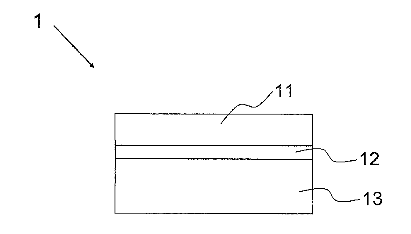
[0071]FIG. 7 is a birds-eye view schematically showing a device structure of a memory cell array 3 used in a nonvolatile semiconductor memory device according to one embodiment of the present invention (hereinafter, referred to as the “device of the present invention” occasionally). In addition, a substantial part is overdrawn for convenience of the description in the following drawings, so that a dimensional ratio of each part of an element does not always coincide with an actual dimensional ratio in some cases.

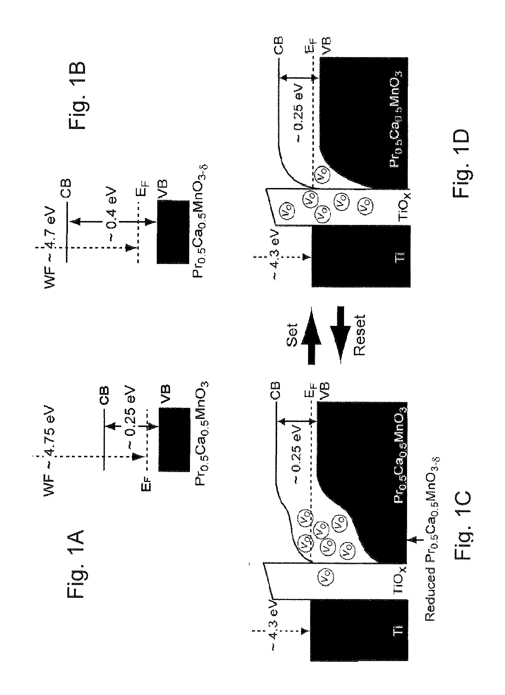
[0072]As shown in FIG. 7, the memory cell array 3 has a cross-point structure in which the above-described variable resistive elements 1 each including a lower electrode (second electrode) 13 formed on an interlayer insulation film 16 (not shown) formed on a Si substrate 10 (not shown), an upper electrode (first electrode) 11 composed of electrodes 17 and 18, and a metal oxide film 12 (12a) having a perovskite structure, are arranged in row and column directions in the form ...

second embodiment

[0111]The device of the present invention can further increase its capacity by employing a three-dimensionally-multilayered memory cell array configuration. FIG. 22 shows a circuit configuration diagram of a memory cell array 5 in which the memory cell arrays 3 shown in FIG. 7 are multilayered. The memory cell array 5 is provided in such a manner that the four memory cell arrays 3 in which the memory cells are specified by the four word lines and the eight bit lines (4×8) are laminated in a third direction (Z direction) perpendicular to the word lines and the bit lines.

[0112]Among the word lines W11 to W44 extending in the row direction (X direction), the word lines arranged in the same position in the column direction (Y direction) and in the different positions in the third direction are connected to any one of selection lines w1 to w4 extending in the common row direction through corresponding transistors in a transistor array ST1. The transistors in the transistor array ST1 are ...


PUM


Abstract

A memory cell array having a 1R structure is composed of nonvolatile variable resistive elements each including a variable resistor formed of a metal oxide film whose resistance changes depending on an oxygen concentration in the film, and first and second electrodes sandwiching the variable resistor. The first electrode and the variable resistor form a rectifier junction through a rectifier junction layer composed of an oxide layer and a layer (oxygen depletion layer) of the metal oxide film having an oxygen concentration lower than a stoichiometric composition. The oxygen moves between the first electrode and the metal oxide film when a voltage is applied, and a thickness of the oxygen depletion layer changes, so that the resistance of the metal oxide film changes and the rectifying properties are provided. A thickness of the oxygen depletion layer is set to allow the variable resistive element to show the sufficient rectifying properties.

Description

CROSS REFERENCE TO RELATED APPLICATION[0001]This Nonprovisional application claims priority under 35 U.S.C. §119(a) on Patent Application No. 2010-148216 filed in Japan on 29 Jun., 2010 the entire contents of which are hereby incorporated by reference.BACKGROUND OF THE INVENTION[0002]1. Field of the Invention[0003]The present invention relates to a nonvolatile semiconductor memory device provided in such a manner that nonvolatile variable resistive elements each having a first electrode, a second electrode, and a variable resistor of a metal oxide film sandwiched by the electrodes are arranged in the form of a matrix, and more particularly it relates to a nonvolatile semiconductor memory device provided with a cross-point type memory cell array having a 1R structure in which the variable resistive element has rectifying properties.[0004]2. Description of the Related Art[0005]In tandem with the penetration of a mobile device such as a portable electric device, a flash memory has been...

Claims


Application Information

Patent Timeline
IPC IPC(8): G11C11/00H01L45/00
CPCG11C11/16H01L27/2481G11C13/0097H01L45/12H01L45/1641H01L45/1675H01L27/249G11C2213/51G11C2213/71G11C2213/72G11C2213/73H01L45/08H01L45/1233H01L45/147G11C13/0069G11C11/1659G11C11/161H10B63/845H10B63/84H10N70/24H10N70/801H10N70/826H10N70/8836H10N70/041H10N70/063
Inventor AWAYA, NOBUYOSHITAMAI, YUKIOSAWA, AKIHITO
Owner SHARP KK
Why Eureka
Try Eureka