Organic electroluminescence device and method for producing organic electroluminescence device

a technology of electroluminescence device and organic electroluminescence, which is applied in the direction of thermoelectric device junction material, semiconductor device, electrical apparatus, etc., can solve the problems of reducing the luminescent efficiency of the device, deteriorating the electron injecting layer of the device, and device having to be driven at a high voltage, so as to reduce the reflectivity of the zinc oxide layer and the reflectivity of the adjacent organic compound layer, the effect of preventing leakage curren

Active Publication Date: 2012-01-19
IDEMITSU KOSAN CO LTD
View PDF5 Cites 67 Cited by
  • Summary
  • Abstract
  • Description
  • Claims
  • Application Information

AI Technical Summary

Benefits of technology

[0074]Since the zinc oxide layer can be formed by a resistance-heating or electron-beam vacuum evaporation method, damages on the layers formed of organic compounds (organic compound layers, e.g., the electron injecting layer, the hole injecting layer and the like), which is located adjacent to the zinc oxide layer can be restrained. For instance, in film-formation of the transparent conductive oxides such as ITO on the organic compound layers, a sputtering process is typically required. Consequently, damages on the organic compound layers by plasma are unavoidable.
[0075]When the zinc oxide layer is formed by the vacuum evaporation method, the formed film is coarser than a film formed by a sputtering method and the like. Consequently, a reflectivity of the zinc oxide layer is decreased. Herein, the reflectivity of the zinc oxide layer in a visible light region is in a range from 1.6 to 2.0, preferably in a range from 1.6 to 1.8. In contrast, a reflectivity of IZO (indium-zinc oxide), which is used for the transparent conductive film or the like, is in a range from 2.0 to 2.2 in the visible light region. This reflectivity is largely different from the reflectivity of the organic compound layer formed by an evaporation method.
[0076]Thus, by forming the zinc oxide layer by the vacuum evaporation method, a difference between the reflectivity of the zinc oxide layer and the reflectivity of the adjacent organic compound layers is lessened, thereby efficiently acquiring light from the first emitting unit and the second emitting unit which sandwich the intermediate unit therebetween.
[0077]Specific resistance of the zinc oxide layer at room temperature is in a range from 1 Ω·cm to 1×10⁵ Ω·cm, preferably in a range from 1×10² Ω·cm to 1×10⁵ Ω·cm. Leak current can be prevented by this specific resistance. The leak current herein indicates that, when a plurality of organic EL devices are located adjacent to each other, for instance, in a planar direction of the substrate as an emission source of a display panel, a current flows through the intermediate unit into an organic EL device not expected to emit light, resulting in emission of the organic EL device. In contrast, since specific resistance of IZO (indium-zinc oxide) at room temperature is 1×10⁻⁴ Ω·cm order, the specific resistance of IZO is sufficiently small relative to that of zinc oxide. As a result, leak current is likely to occur.
[0078]A thickness of the zinc oxide layer is preferably in a range from 3 nm to 20 nm, more preferably in a range from 3 nm to 10 nm. Leak current can be further prevented within this range.
[0079]The zinc oxide layer provided as the intermediate unit can prevent leak current, so that a clear image display is possible, for instance, when the organic EL device is used as the emission source for display.

Problems solved by technology

However, in the sputtering process, it is considered that a neutral particle and a charged particle of high speed (tens of electron volts (eV) or more) which are derived from generated plasma cause damages to an organic substance, thereby deteriorating the electron injecting layer of the device.
Consequently, the device has to be driven at a high voltage and luminescent efficiency thereof is reduced.
In Patent Literature 5 in which lead oxide is used as the interface layer, since lead oxide is an oxide having a low melting point, satisfactory drive durability could not be obtained.
When the charge generating layer disclosed in Patent Literature 6 is employed as the intermediate unit, visible light is absorbed by the charge transfer complex, resulting in reduction in luminescent efficiency.

Method used


Image

  • Organic electroluminescence device and method for producing organic electroluminescence device
  • Organic electroluminescence device and method for producing organic electroluminescence device
  • Organic electroluminescence device and method for producing organic electroluminescence device

Examples


first exemplary embodiment

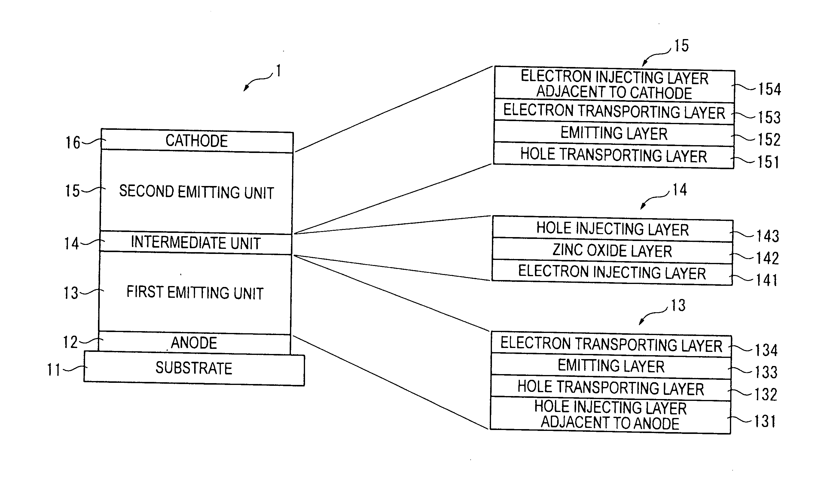
[0052]The tandem-type organic EL device includes the plurality of emitting units, e.g., a first emitting unit and a second emitting unit, as follows:

[0053]anode / first emitting unit / intermediate unit / second emitting unit / cathode.

[0054]In the first exemplary embodiment, a tandem-type organic EL device 1 arranged as shown in FIG. 1 is exemplarily described. The organic EL device 1 is provided by laminating an anode 12, a first emitting unit 13, an intermediate unit 14, a second emitting unit 15 and a cathode 16 on a substrate 11 in this sequence. As shown in FIG. 1, the first emitting unit 13, the intermediate unit 14 and the second emitting unit 15 are respectively provided with a plurality of layers. The arrangements thereof are as follows.

[0055]The first emitting unit 13:[0056]a hole injecting layer 131 adjacent to the anode[0057]a hole transporting layer 132[0058]an emitting layer 133[0059]an electron transporting layer 134

[0060]The intermediate unit 14:[0061]an electron injecting ...

second exemplary embodiment

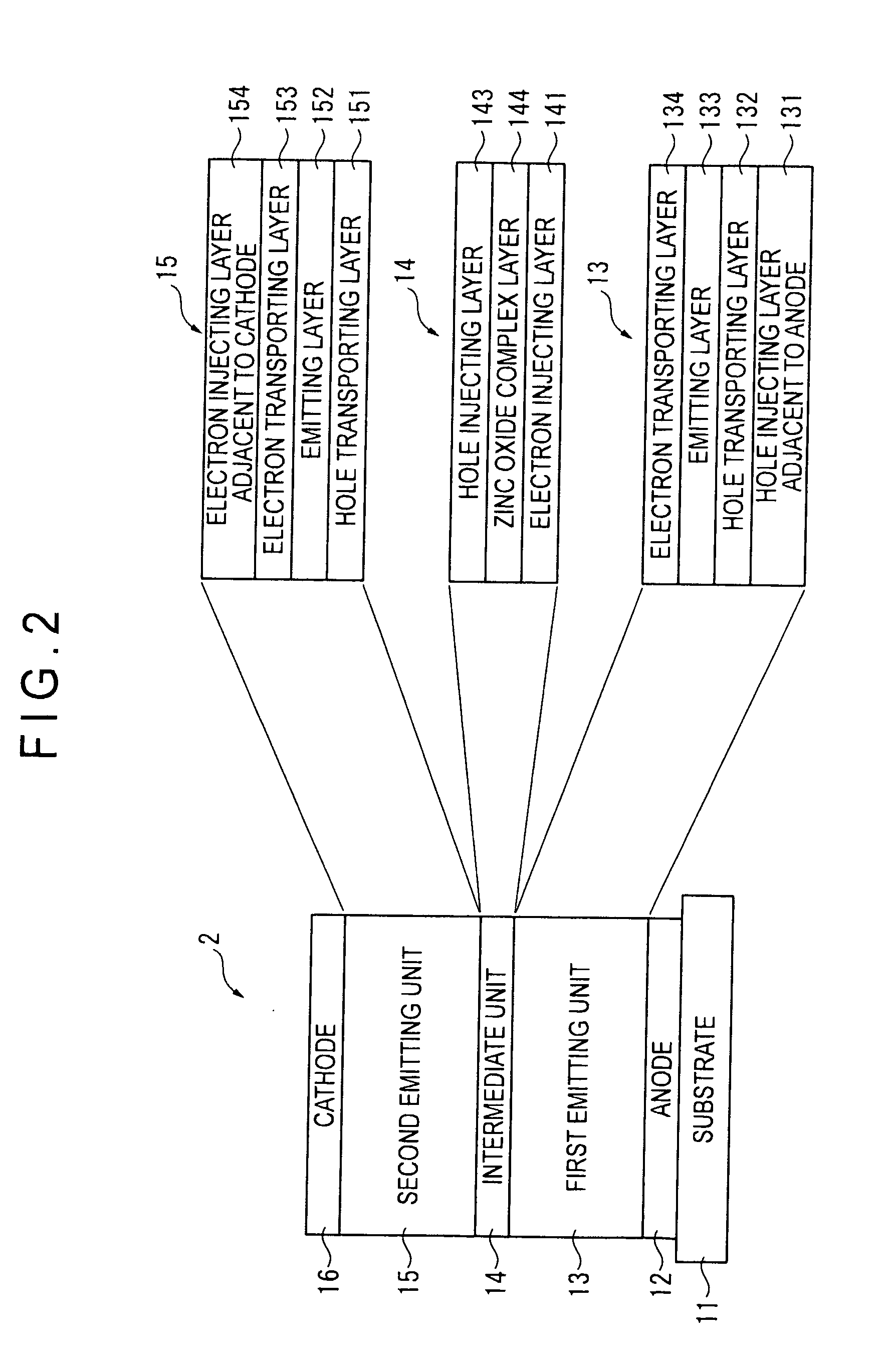
[0204]Next, a second exemplary embodiment is described below.

[0205]In the description of the second exemplary embodiment, the same components as those in the first exemplary embodiment are denoted by the same reference signs and names to simplify or omit an explanation of the components. In the second exemplary embodiment, the same materials and compounds as described in the first exemplary embodiment are usable.

[0206]As shown in FIG. 2, an organic EL device 2 according to the second exemplary embodiment is the same as the organic EL device 1 except that the zinc oxide layer 141 in the intermediate unit 14 of the organic EL device 1 is replaced by a zinc-containing complex oxide layer 144.

(Intermediate Unit)

[0207]The intermediate unit supplies electrons to the first emitting unit and supplies holes to the second emitting unit.

[0208]The intermediate unit includes the zinc-containing complex oxide layer, the electron injecting layer on the zinc-containing complex oxide layer near the ...

third exemplary embodiment

[0238]Next, a third exemplary embodiment is described below.

[0239]In the description of the third exemplary embodiment, the same components as those in the first exemplary embodiment are denoted by the same reference signs and names to simplify or omit an explanation of the components. In the third exemplary embodiment, the same materials and compounds as described in the first exemplary embodiment are usable.

[0240]As shown in FIG. 3, an organic EL device 3 according to the third exemplary embodiment, includes three emitting units and two intermediate units.

[0241]The organic EL device 3 is provided by laminating the anode 12, the first emitting unit 13, a first intermediate unit 14A, the second emitting unit 15, a second intermediate unit 14B, a third emitting unit 17 and the cathode 16 on the substrate 11 in this sequence.

[0242]The first emitting unit 13 and the second emitting unit 15 in the third exemplary embodiment is essentially the same as those in the first exemplary embodim...


PUM


Abstract

An organic electroluminescence device includes: an anode; a cathode opposed to the anode; and a plurality of emitting units including at least a first emitting unit and a second emitting unit. The plurality of emitting units each includes: an emitting layer; and an intermediate unit between the first emitting unit and the second emitting unit. The intermediate unit includes an electron injecting layer, a zinc oxide layer and a hole injecting layer in this sequence from the anode. The electron injecting layer contains an electron donating material and is adjacent to the first emitting unit. The hole injecting layer contains an organic electron accepting material and is adjacent to the second emitting unit.

Description

[0001]The entire disclosure of Japanese Patent Applications No. 2010-161273 filed Jul. 16, 2010, and No. 2010-192603 filed Aug. 30, 2010, are expressly incorporated by reference herein.TECHNICAL FIELD[0002]The present invention relates to an organic electroluminescence device and a manufacturing method thereof.BACKGROUND ART[0003]There has been known an organic electroluminescence device (hereinafter, referred to as an “organic EL device”) that includes an emitting unit (in which an emitting layer is included) between an anode and a cathode and emits light using exciton energy generated by a recombination of holes and electrons that have been injected into the emitting layer.[0004]Recently, an arrangement of the organic EL device having a plurality of the emitting units laminated via an intermediate unit and connected in series has been studied for improving luminescent efficiency and lifetime of the organic EL device. Such a device arrangement is occasionally called a tandem-type.[...

Claims


Application Information

Patent Timeline
Patent Type & Authority Applications(United States)
IPC IPC(8): H01L51/52H01L51/56
CPCH01L51/5278H01L27/3211H10K59/35H10K50/131H10K50/19
Inventor ENDO, JUNHOSOKAWA, CHISHIO
Owner IDEMITSU KOSAN CO LTD
Why Eureka
Try Eureka