Liquid Chemical for Forming Protecting Film

a technology of liquid chemical and protective film, which is applied in the direction of detergent compounding agent, other chemical processes, cleaning using liquids, etc., can solve the problems of increasing the aspect ratio, the damage to the wafer due to cleaning, and the basicity of the wafer, so as to reduce the capillary force, improve the water repellency, and improve the effect of water repellency

Active Publication Date: 2012-01-26
CENT GLASS CO LTD
View PDF2 Cites 29 Cited by
  • Summary
  • Abstract
  • Description
  • Claims
  • Application Information

AI Technical Summary

Benefits of technology

[0037]A protecting film formed by a liquid chemical of the present invention for forming a protecting film is excellent in water repellency, and therefore reduces the capillary force of an unevenly patterned surface of a wafer, and by extension brings about a pattern collapse-preventing effect. With the use of the liquid chemical, a cleaning step conducted in a process for producing the wafer formed having a finely unevenly patterned surface is improved without lowering throughput. Accordingly, the process for producing the wafer formed having the finely unevenly patterned surface is excellent in productivity.
[0038]The liquid chemical of the present invention for forming the protecting film is adaptable to uneven patterns having aspect ratios expected to rise more and more, for example, to an aspect ratio of not less than 7, and therefore allows cost reduction in producing more sophisticated semiconductor devices. In addition to this, the liquid chemical is adaptable without considerably modifying conventional apparatuses, which results in being one applicable in production of various kinds of semiconductor devices.
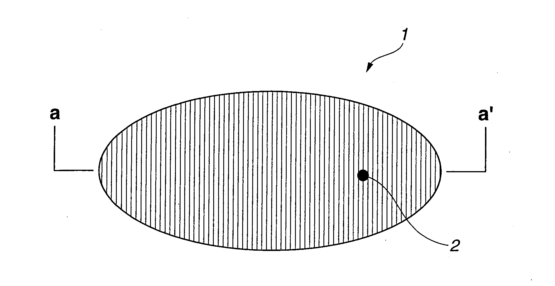
[0039]FIG. 1 A schematic plan view of a wafer 1 whose surface is made into a surface having a finely uneven pattern 2.
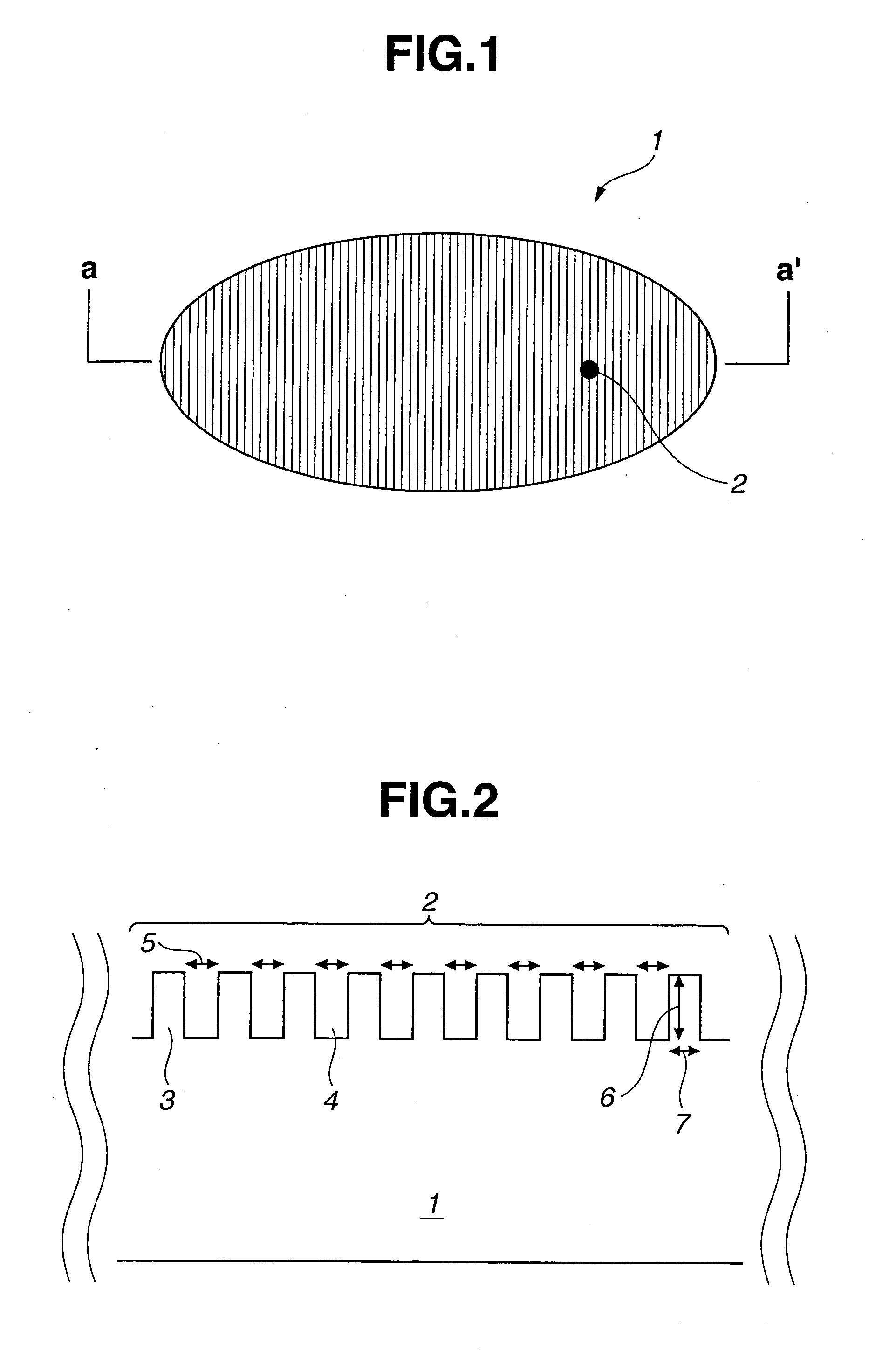
[0040]FIG. 2 A view showing a part of a-a cross section of FIG. 1.
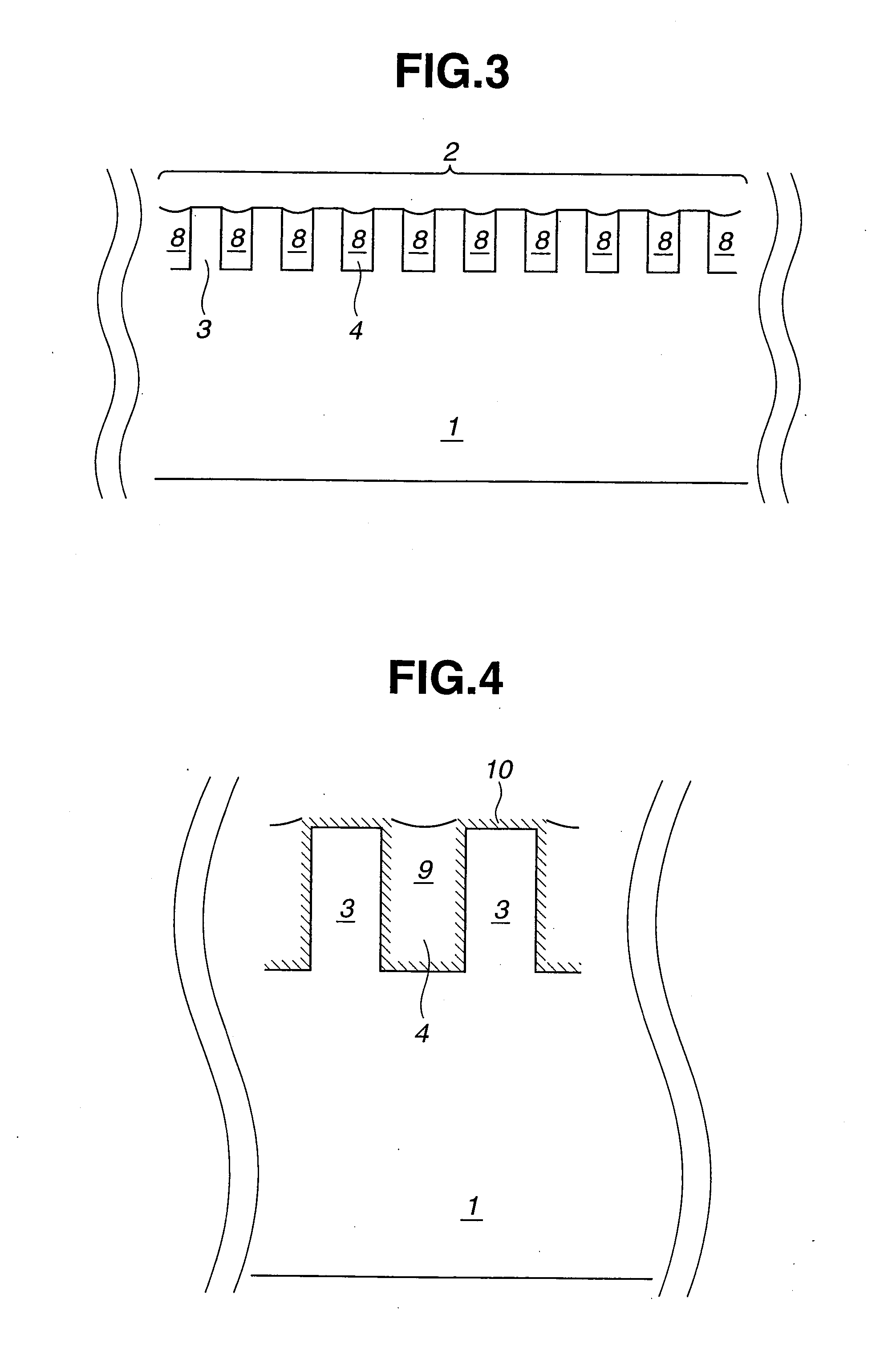
[0041]FIG. 3 A schematic view showing a liquid chemical 8 for forming a protecting film is retained in recessed portions 4 in a cleaning step.
[0042]FIG. 4 A schematic view showing a condition where a water-based cleaning liquid is retained in the recessed portions 4 on which the protecting film is formed.

Problems solved by technology

On the other hand, in cleaning conventionally performed with a mixed ammonia cleaning agent, damages to the wafer due to its basicity are getting serious with the trend toward micro-patterning for circuits.
With this, problems about the damages to the wafer due to cleaning have been solved; however, problems due to an aspect ratio increased with the trend toward micro-processing in the semiconductor devices have become obvious.
In other words, a phenomenon where the pattern collapses when a gas-liquid interface passes through the pattern is brought about after cleaning or rinsing to largely reduce the yield, which has become a significant problem.
This method is effective for preventing the pattern collapse; however, a solvent having small γ such as 2-propanol and the like is also small in normal contact angle, which results in the trend to increase cos θ. It is therefore said that there are limitations to adaptable patterns, for example, an aspect ratio of not higher than 5.
However, the thus disclosed technique cannot be applied to the present object because: the technique is directed to the resist pattern or for reforming a resist itself; and a final removal together with the resist is possible so as not to need the assumption about a method of removing a treatment agent after drying.
However, any of these is difficult to apply to a mass-producing process because of its poorer throughput than in conventional cleaning steps, though effective to some extent.

Method used


Image

  • Liquid Chemical for Forming Protecting Film
  • Liquid Chemical for Forming Protecting Film
  • Liquid Chemical for Forming Protecting Film

Examples


example 1

[0156](1) Preparation of Liquid Chemical for Forming Protecting Film

[0157]1 g of hexamethyldisilazane [(H3C)3Si—NH—Si(CH3)3] as a silicon compound A, 0.1 g of trimethylsilyl trifluoroacetate [(CH3)3Si—OC(O)CF3] as an acid A, 98.9 g of propylene glycol monomethyl ether acetate (PGMEA) were mixed thereby obtaining a liquid chemical for forming a protecting film. Incidentally, it was confirmed that the total quantity of the water content in the starting material for the liquid chemical was not more than 5000 mass ppm relative to the total quantity of the raw material. A water content was removed from the liquid chemical by molecular sieve 4 A (produced by UNION SHOWA K.K.). Thereafter, a metal impurity was removed from the liquid chemical by an ion-exchange resin (IonKleen™ SL Purifier produced by Pall Corporation), followed by removing particles from the liquid chemical by filtration separation (Optimizer produced by Nihon Entegris K.K.), thereby conducting purification. The water con...

examples 2 to 56

[0163]The surface treatment was conducted on the wafer upon suitably modifying the conditions of Example 1, such as the silicon compound A, the concentration of the silicon compound A, the acid A, the organic solvent, the for forming the protecting film and the like. Then, evaluation was performed thereon. Results of them are shown in Tables 1 and 2.

TABLE 2Liquid Chemical for forming Protecting FilmStarting MaterialConcentration of SiliconCompound ASilicon Compound A[mass %]Acid AOrganic SolventExample 28(H3C)2Si(H)—NH—Si(H)(CH3)21(CH3)3Si—OC(O)CF3HFE-7100 / PGMEAExample 29(H3C)3Si—NH—Si(CH3)31(CH3)3Si—OC(O)CF3PGMEAExample 30(H3C)2Si(H)—NH—Si(H)(CH3)21(CH3)3Si—OC(O)CF3PGMEAExample 31(H3C)3Si—NH—Si(CH3)31(CH3)3Si—OC(O)CF3PGMEAExample 32(H3C)2Si(H)—NH—Si(H)(CH3)21(CH3)3Si—OC(O)CF3PGMEAExample 33(H3C)3Si—NH—Si(CH3)31(CH3)3Si—OC(O)CF3PGMEAExample 34(H3C)2Si(H)—NH—Si(H)(CH3)21(CH3)3Si—OC(O)CF3PGMEAExample 35C6H5Si(CH3)2—NH—Si(CH3)2C6H51(CH3)3Si—OC(O)CF3PGMEAExample 36C6H5Si(CH3)2—NH—Si(CH3...

example 57

[0177]The procedure was the same as Example 1 with the exception that the liquid chemical for forming the protecting film, containing trimethylsilyl trifluoroacetate as the acid A, hexamethyldisilazane as the silicon compound A and PGMEA as the organic solvent, was obtained by mixing 1 g of hexamethyldisilazane [(H3C)3Si—NH—Si(CH3)3] as a silicon compound B, 0.1 g of trifluoroacetic anhydride [{CF3C(O)}]2O] as the acid B and 98.9 g of PGMEA as the organic solvent and then reacting them. Hexamethyldisilazane contained in the liquid chemical of the present example is the silicon compound B which is not consumed in the reaction for obtaining the acid A, and the components thereof are able to function as the silicon compound A. As an evaluation result, the contact angle after the surface treatment was 82° as shown in Table 3 and therefore exhibited a water repellency-providing effect. Furthermore, the capillary force when water was retained was 0.4 MN / m2 and therefore low. Additionally,...


PUM

PropertyMeasurementUnit
water-repellentaaaaaaaaaa
aspect ratioaaaaaaaaaa
poweraaaaaaaaaa

Abstract

Disclosed is a liquid chemical for forming a water-repellent protecting film at least on a surface of a recessed portion of an uneven pattern at the time of cleaning a wafer having a finely uneven pattern at its surface and containing silicon at least a part of the uneven pattern. This liquid chemical contains a silicon compound A represented by the general formula: R1aSi(H)bX4-a-b and an acid A, the acid A being at least one selected from the group consisting of trimethylsilyl trifluoroactate, trimethylsilyl trifluoromethanesulfonate, dimethylsilyl trifluoroactate, dimethylsilyl trifluoromethanesulfonate, butyldimethylsilyl trifluoroactate, butyldimethylsilyl trifluoromethanesulfonate, hexyldimethylsilyl trifluoroacetate, hexyldimethylsilyl trifluoromethanesulfonate, octyldimethylsilyl trifluoroactate, octyldimethylsilyl trifluoromethanesulfonate, decyldimethylsilyl trifluoroacetate and decyldimethylsilyl trifluoromethanesulfonate.

Description

TECHNICAL FIELD[0001]The present invention relates to a technique of cleaning a substrate (a wafer) in production of semiconductor devices or the like which technique aims to improve the production yield of devices having such a circuit pattern as to be particularly fine and particularly high in aspect ratio, and more particularly to a liquid chemical for forming a water-repellent protecting film which liquid chemical aims to improve a cleaning step which tends to induce the collapse of an uneven pattern in the wafer having at its surface a finely uneven pattern.BACKGROUND OF THE INVENTION[0002]Semiconductor devices for use in networks or digital household electric appliances are being further desired to be sophisticated, multifunctional, and low in power consumption. Accordingly, the trend toward micro-patterning for circuits has been developed, with which micro-sizing of particles has advanced to cause reduction in production yield. As a result of this, a cleaning step for the pur...

Claims


Application Information

Patent Timeline
Patent Type & Authority Applications(United States)
IPC IPC(8): B08B7/00C09K3/18
CPCC09K3/18C11D1/82C11D3/162C11D11/0047B08B3/08B08B3/10H01L21/02057H01L21/02082
Inventor KUMON, SOICHISAIO, TAKASHIARATA, SHINOBUSAITO, MASANORIRYOKAWA, ATSUSHIYAMADA, SHUHEINANAI, HIDEHISAAKAMATSU, YOSHINORI
Owner CENT GLASS CO LTD
Why Eureka
Try Eureka