Film for flip chip type semiconductor back surface, dicing tape-integrated film for semiconductor back surface, process for producing semiconductor device, and flip chip type semiconductor device

a technology of flip chip and back surface, which is applied in the direction of adhesive types, instruments, transportation and packaging, etc., can solve the problems of increasing the number of processing steps, increasing the production cost, and damaging the semiconductor chips, so as to achieve suppressed or prevented damage to the semiconductor element, excellent visibility, and effective prevention of adverse influences

Inactive Publication Date: 2012-01-26
NITTO DENKO CORP
View PDF2 Cites 9 Cited by
  • Summary
  • Abstract
  • Description
  • Claims
  • Application Information

AI Technical Summary

Benefits of technology

[0029]According to the film for flip chip type semiconductor back surface of the invention, since the film is formed on the back surface of a semiconductor element flip chip-connected on an adherend, the film exerts the function of protecting the semiconductor element. Moreover, according to the film for flip chip type semiconductor back surface of the invention, since a light transmittance at a wavelength of 532 nm or 1064 nm is 20% or less and a contrast between a marking part and the part other than the marking part after laser marking is 20% or more, various kinds of information excellent in visibility can be imparted by laser marking, while the semiconductor element is effectively prevented from being adversely influenced.
[0030]Moreover, according to the dicing tape-integrated film for semiconductor back surface of the invention, the dicing tape and the film for flip chip type semiconductor back surface are formed in an integrated form, and therefore, the dicing tape-integrated film for semiconductor back surface can also be provided for a dicing step of dicing a semiconductor wafer to prepare a semiconductor element or the subsequent picking-up step. As a result, a step of attaching the film for semiconductor back surface alone (attaching step of the film for semiconductor back surface) is not required. Furthermore, in the subsequent dicing step and pick-up step, since the film for semiconductor back surfa

Problems solved by technology

However, protecting the back surface of a semiconductor chip with a protective film requires an additional step of attaching a protective film to the back surface of the semiconductor chip obtained in a dicing step.
As a result, the number

Method used

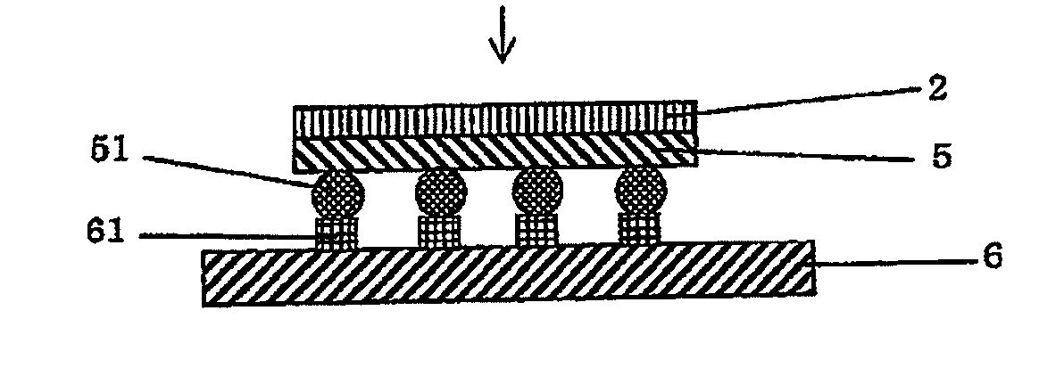
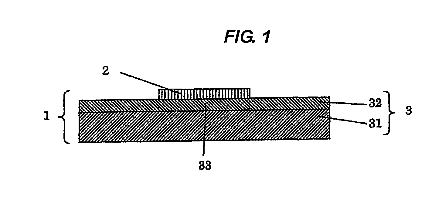
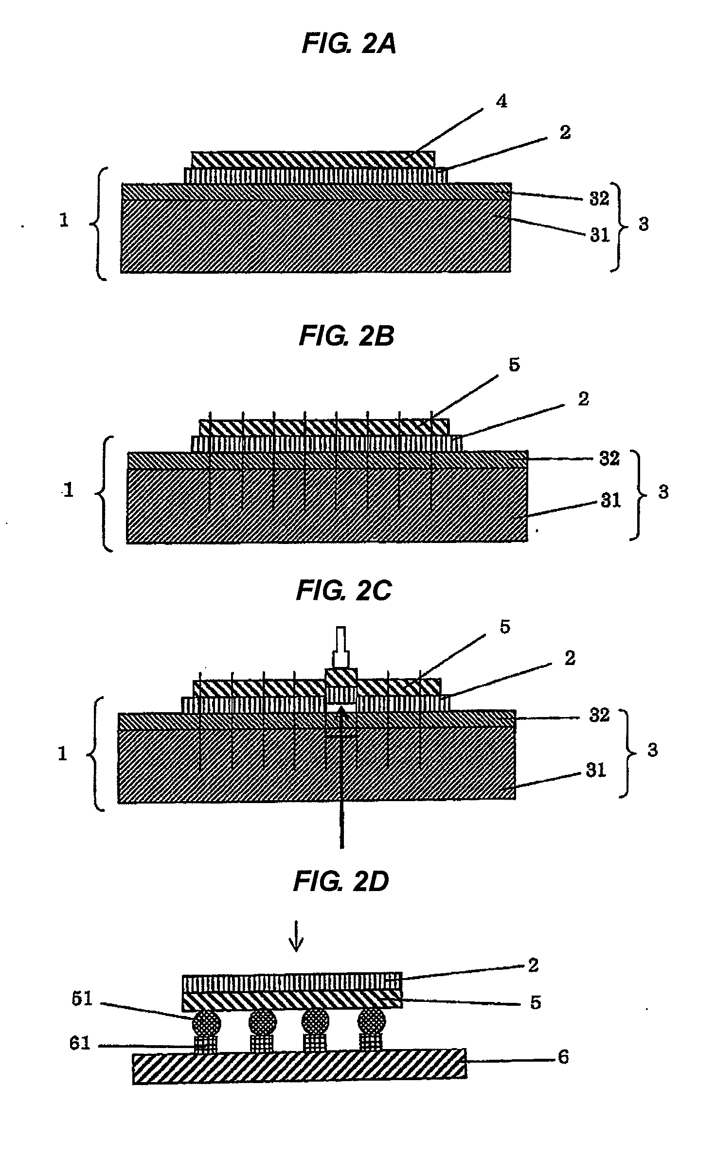

Image

  • Film for flip chip type semiconductor back surface, dicing tape-integrated film for semiconductor back surface, process for producing semiconductor device, and flip chip type semiconductor device
  • Film for flip chip type semiconductor back surface, dicing tape-integrated film for semiconductor back surface, process for producing semiconductor device, and flip chip type semiconductor device
  • Film for flip chip type semiconductor back surface, dicing tape-integrated film for semiconductor back surface, process for producing semiconductor device, and flip chip type semiconductor device

Examples


example 1

Preparation of Film for Flip Chip Type Semiconductor Back Surface

[0176]113 parts of an epoxy resin (trade name “EPIKOTE 1004” manufactured by JER Co., Ltd.), 121 parts of a phenol resin (trade name “MIREX XLC-4L” manufactured by Mitsui Chemicals, Inc.), 246 parts of a spherical silica (trade name “SO-25R” manufactured by Admatechs Company Limited), 18 parts of a coloring agent (trade name “Oil Black 860” manufactured by Orient Chemical Industries Co., Ltd.) (content based on 100 parts of resin composition: 3 parts) based on 100 parts of an acrylic acid ester-based polymer (trade name “PARACRON W-197CM” manufactured by Negami Chemical Industrial Co., Ltd.) containing ethyl acrylate and methyl methacrylate as main components were dissolved in methyl ethyl ketone to prepare a solution of an adhesive composition having a solid concentration of 23.6% by weight.

[0177]The solution of the adhesive composition was applied on a releasably treated film, as a release liner (separator), composed...

example 2

[0191]In Example 2, a dicing tape-integrated film for semiconductor back surface according to Example 2 was obtained in the same manner as in Example 1 except that the coloring agent was changed to a black pigment (#47 manufactured by Mitsubishi Chemical Corporation, amount to be added: 3 parts (content based on 100 parts by weight of resin composition: 0.5 parts)).

example 3

Preparation of Wafer Adhesive Layer

[0239]21 parts of an epoxy resin (trade name “EPIKOTE 1004” manufactured by JER Co., Ltd.), 22 parts of a phenol resin (trade name “MIREX XLC-4L” manufactured by Mitsui Chemicals, Inc.), and 77 parts of a spherical silica (trade name “SO-25R” manufactured by Admatechs Company Limited) based on 100 parts of an acrylic acid ester-based polymer (trade name “PARACRON W-197CM” manufactured by Negami Chemical Industrial Co., Ltd.) containing ethyl acrylate and methyl methacrylate as main components were dissolved in methyl ethyl ketone to prepare a solution of an adhesive composition having a solid concentration of 23.6% by weight.

[0240]The solution of the adhesive composition was applied on a releasably treated film, as a release liner (separator), composed of a polyethylene terephthalate film having a thickness of 50 μm, which had been subjected to a silicone-releasing treatment, and then dried at 130° C. for 2 minutes to prepare a film A composed of a...


PUM

PropertyMeasurementUnit
Fractionaaaaaaaaaa
Fractionaaaaaaaaaa
Fractionaaaaaaaaaa

Abstract

The present invention relates to a film for flip chip type semiconductor back surface to be formed on a back surface of a semiconductor element flip chip-connected onto an adherend, the film having a light transmittance at a wavelength of 532 nm or 1064 nm of 20% or less, and having a contrast between a marking part and a part other than the marking part after laser marking of 20% or more.

Description

FIELD OF THE INVENTION[0001]The present invention relates to a film for flip chip type semiconductor back surface and a dicing tape-integrated film for semiconductor back surface. The film for flip chip type semiconductor back surface is used for the purposes of protecting a back surface of a semiconductor element such as a semiconductor chip and enhancing strength thereof and the like. Also, the invention relates to a process for producing a semiconductor device using a dicing tape-integrated film for semiconductor back surface and a flip chip type semiconductor device.BACKGROUND OF THE INVENTION[0002]Recently, thinning and miniaturization of a semiconductor device and its package have been increasingly demanded. Therefore, as the semiconductor device and its package, flip chip type semiconductor devices in which a semiconductor element such as a semiconductor chip is mounted (flip chip-connected) on a substrate by means of flip chip bonding have been widely utilized. In such flip ...

Claims


Application Information

Patent Timeline
IPC IPC(8): H01L23/48B32B3/00H01L21/50
CPCC09J163/00H01L21/561H01L21/6835H01L23/293H01L23/3114H01L23/3157H01L23/544H01L24/13H01L24/16H01L24/32H01L24/81H01L24/83H01L2221/68327H01L2221/68336H01L2221/68377H01L2221/68381H01L2223/54406H01L2223/54413H01L2223/54433H01L2223/54486H01L2224/131H01L2224/16258H01L2224/16268H01L2224/2919H01L2224/73204H01L2224/81002H01L2224/81193H01L2224/81815H01L2224/8191H01L2224/831H01L2224/83862H01L2924/01013H01L2924/01029H01L2924/0103H01L2924/01038H01L2924/01051H01L2924/01056H01L2924/01079H01L2924/01082H01L2924/01005H01L2924/01006H01L2924/0102H01L2924/01023H01L2924/01024H01L2924/01033H01L2924/01042H01L2924/01045H01L2924/01047H01L2924/0105H01L2924/01074H01L2924/01075H01L2924/014H01L2224/16225H01L2224/13111H01L2224/13144H01L2224/13147H01L2924/0001Y10T428/24802H01L2924/3512H01L2924/00H01L2924/00014H01L2924/01083H01L2224/13099H01L2924/15787H01L2924/15788
Inventor TAKAMOTO, NAOHIDESHIGA, GOJIASAI, FUMITERU
Owner NITTO DENKO CORP
Why Eureka
Try Eureka