Multipulse system for writing waveguides, gratings, and integrated optical circuits

a technology of integrated optical circuits and waveguides, applied in optics, instruments, optical elements, etc., can solve the problems of limited attempts to inscribe grating structures into laser-written waveguides, no evidence of applicability, and only successful techniques, so as to improve the accuracy and speed of fabrication. , the effect of reducing the cos

Active Publication Date: 2012-02-16
HERMAN +2
View PDF7 Cites 40 Cited by
  • Summary
  • Abstract
  • Description
  • Claims
  • Application Information

AI Technical Summary

Benefits of technology

[0028]The method and system of the present invention enables 3-D fabrication and integration of sensing and filtering functions in 1-D, 2-D, and 3-D optical circuits. Because one laser writing step may be employed, the method of the present invention simplifies the fabrication process which leads to faster fabrication, lower cost and enables highly versatile optical devices or systems to be designed and fabricated. Further, the method and system apply weaker multiple pulse interactions to build up refractive index changes more gently over a number of laser pulses that potentially reduce stress, shock, defect formation, and other deleterious effects. Multiple pulses further offer substantial control of voxel-to-voxel overlap, physical size, shape, strength of refractive index change, and other optical parameters, thus enabling new means to control the relative. AC and DC components of the waveguide effective refractive index, and thereby may be used to tune Bragg grating spectral features in shape, strength, polarization dependence, radiation loss, and dispersion. With appropriate matching of laser exposure conditions to the optical properties of transparent or near-transparent substrates, the method of the present invention lends application to a broad range of materials, including but not limited to glasses, crystals, polymers and multi-layered or multi-structured materials.

Problems solved by technology

Several methods have been applied to fabricate Bragg and long-period gratings in optical fibers or planner waveguide circuits, but there has been only limited demonstration of such structures in three-dimensional (“3-D”) optical circuits.
However, these techniques have only been demonstrated to be successful in a pre-existing waveguide (optical fiber) with no evidence of applicability in PLC or 3-D photonic circuits.
However, despite the work described above, there have only been limited attempts to inscribe grating structures into such laser-written waveguides.

Method used


Image

  • Multipulse system for writing waveguides, gratings, and integrated optical circuits
  • Multipulse system for writing waveguides, gratings, and integrated optical circuits
  • Multipulse system for writing waveguides, gratings, and integrated optical circuits

Examples


example 1

[0110]A grating waveguide fabrication method and system to produce modulation of refractive index and / or other waveguide properties by periodic or modified periodic modulation of a energy source (e.g., a laser) was demonstrated. This method can be applied to both low and high repetition rate laser systems and continuous wave laser systems. Low-loss and high-strength Bragg grating waveguides were fabricated in fused silica glass with a commercial high-repetition rate, fiber-amplified laser. The method can easily be adapted to other laser sources and materials.

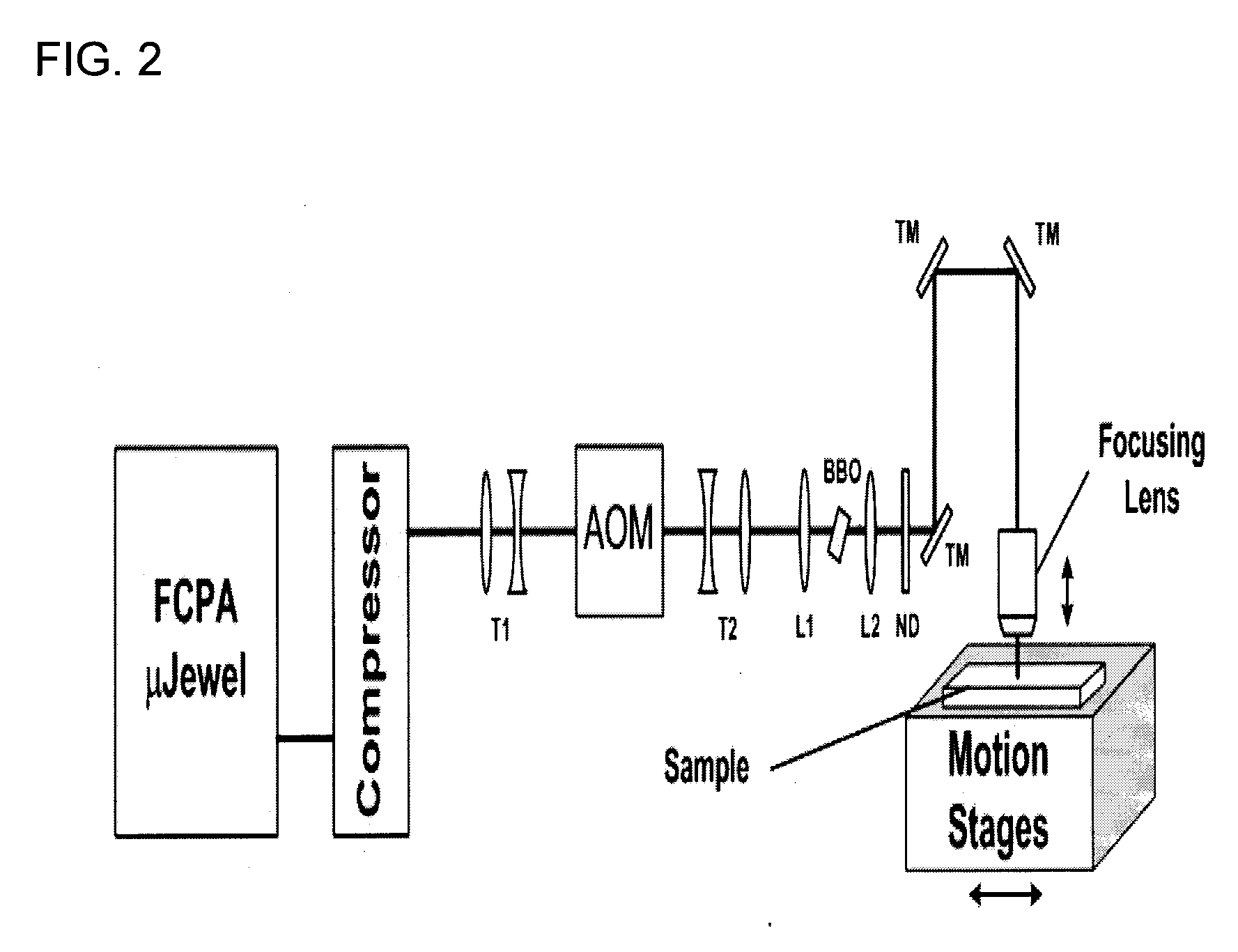
[0111]FIG. 2 illustrates a system in accordance with an embodiment of an aspect of the present invention. A commercial amplified fiber laser (IMRA America™, model λJewel-400) provides 1045 nm wavelength of ˜400 fs pulse duration from an external compressor, with tuneable repetition rate from 100 kHz to 5 MHz and with M2 beam quality value of ˜1.3. In the present example, a 500 kHz repetition rate was applied, but other frequenci...

example 2

[0129]This example is an extension of Example 1 which demonstrates the flexibility of the present GW formation method in controlling waveguide properties and integrating multiple GW devices to form highly stable optical systems.

[0130]FIG. 11 illustrates the transmission and reflection spectra of several grating waveguide devices formed in series in a straight line in bulk fused silica glass. Each waveguide section was 8 mm long and formed with an AOM modulation rate of 500 Hz and a fixed duty cycle of 60%, using laser exposure conditions similar to that described in Example 1. However, the scan speed was varied in three steps of ν=0.2643, 0.2661, and 0.2678 mm / s, yielding three distinct and separated Bragg resonances at λB=1523.1, 1538.3, and 1548.0 nm, that accurately track the expected relationship of λB=2neffΛ=2neffν / f. The grating strengths for all three resonances exceed 20 dB and provide sharp resonances of ˜0.3 nm spectral width (3 dB), indicating facile means for integration...

example 3

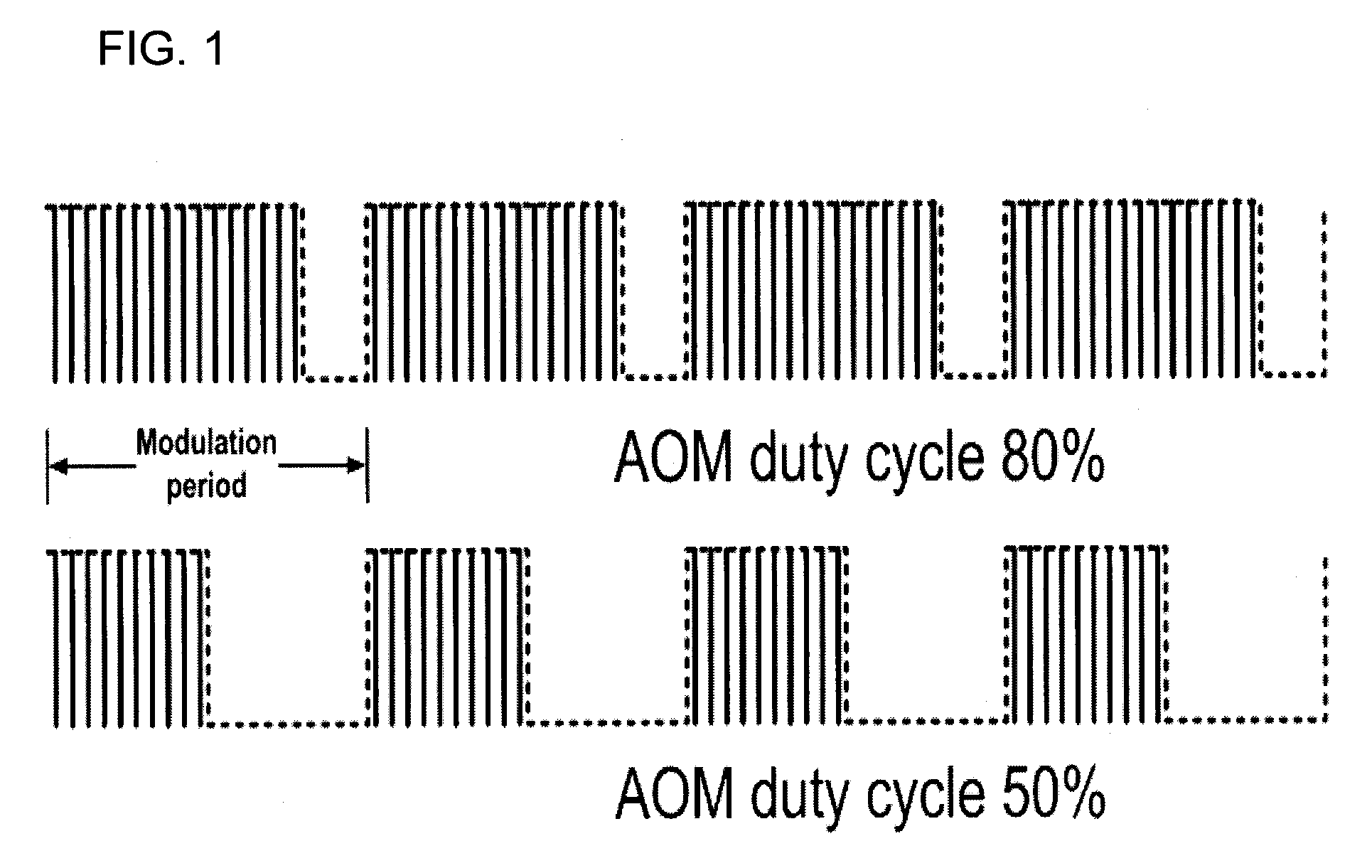
[0139]This example teaches the use of the 0th order diffraction beam from the AOM to form GWs with periodic changes in power level. The embodiment of FIG. 2 is applied with the 0th order diffraction beam of the AOM selected as in FIG. 3 to provide modulated pulse energy variable anywhere within a minimum of ˜45% to a maximum of 100% total laser energy per pulse. For the present case, a square modulation envelope was selected, set to 45% minimum and 100% pulse energy.

[0140]FIG. 4 demonstrates two examples of a similar case of 50% and 100% modulation of pulse energy with external AOM triggering set to 80% and 50% duty cycles for top, middle, and bottom figures, respectively.

[0141]FIG. 15 illustrates the laser power measured in the 0th order AOM diffraction beam as a function of AOM duty cycle. The solid line representation of the data demonstrates the linear control of laser power (or pulse energy or intensity), which intersects the vertical axis at ˜55% maximum power, which is select...


PUM

PropertyMeasurementUnit
Bragg grating lengthaaaaaaaaaa
lengthaaaaaaaaaa
temperaturesaaaaaaaaaa

Abstract

The present invention provides a direct laser writing fabrication method and system for devices having periodic refractive index modulation structures, for example, Bragg gratings. By focusing a modulated pulsed laser beam into a transparent material substrate, a path of laser modified volumes can be formed with modified refractive index compared with the unprocessed material. Modulation of exposure conditions provides periodic or modified periodic waveguide structures such that the waveguide structures exhibit grating responses and can be used for a variety of optical applications, for example, as spectral filters, Bragg reflectors, grating couplers, grating sensors, or other devices. The method enables direct one-step fabrication and integration of periodic or modified periodic refractive-index modulation devices together with other optical waveguiding devices to enable low-cost, multifunctional one-dimensional, two-dimensional or three-dimensional optical circuit fabrication of simple and complex optical systems.

Description

PRIORITY[0001]The present application claims priority from U.S. provisional patent applications nos. U.S. 60 / 895,168 filed Mar. 16, 2007 and U.S. 60 / 969,572 filed Aug. 31, 2007.FIELD OF THE INVENTION[0002]The present invention relates to optics and photonics. In particular, the present invention relates to methods and systems for fabricating waveguides, gratings and integrated optical circuits.BACKGROUND OF THE INVENTION[0003]In optics, gratings with a spatially varying periodic refractive index provide general means of spectral control of light propagation in optical materials. Such refractive index modulation in optical fibers may provide a fiber Bragg grating (“FBG”), widely employed in sensing and Telecom applications as a narrow-band spectral filter. Another manifestation of the fiber-based gratings is the long period grating (“LPG”) which has a much larger period of index modulation compared with FBGs. These grating devices are prominent in current sensing and communication ap...

Claims


Application Information

Patent Timeline
Patent Type & Authority Applications(United States)
IPC IPC(8): G02B6/34C03C25/68
CPCG02B5/1857G02B6/02147G02B6/124G02B6/34G02B2006/12164G02B2006/12171G02B6/13
Inventor HERMAN, PETER R.ZHANG, HAIBINEATON, SHANE MICHAEL
Owner HERMAN
Why Eureka
Try Eureka