Film formation apparatus and film formation method

a film formation apparatus and film technology, applied in the direction of vacuum evaporation coating, electrolysis components, coatings, etc., can solve the problems of significantly impairing affecting and reducing the reliability of transistors using oxide semiconductors. , to achieve the effect of reducing efficient removal of hydrogen in a short time, and reducing the amount of hydrogen on the substrate surfa

Inactive Publication Date: 2012-02-23
SEMICON ENERGY LAB CO LTD
View PDF13 Cites 27 Cited by
  • Summary
  • Abstract
  • Description
  • Claims
  • Application Information

AI Technical Summary

Benefits of technology

[0024]Note that in the case where the substrate heating chamber also serves as a plasma treatment chamber, hydrogen on a substrate surface may be reduced through plasma treatment instead of the above-mentioned heat treatment. The plasma treatment enables treatment at low temperature and efficient removal of hydrogen in a short time, and is particularly effective in removing hydrogen which is strongly bonded to a substrate surface.
[0025]Further, entry of hydrogen from the outside can be suppressed by films between which a transistor is interposed and which block hydrogen. Furthermore, there is need to reduce the effect of desorption and diffusion of hydrogen from a film included in a transistor; for that, a reduction of the hydrogen concentration in the film included in the transistor is effective. In addition, an interface between films might contain hydrogen adsorbed in air; in order to reduce such hydrogen, maximum avoidance of exposure to air is effective. If the exposure to air cannot, however, be avoided, heat treatment is preferably conducted just before film formation at a temperature greater than or equal to 250° C. and less than the strain point of the substrate in an inert atmosphere, a reduced-pressure atmosphere, or a dry air atmosphere. Through this heat treatment, adsorbed hydrogen on a substrate surface can be removed efficiently.
[0026]As described above, a technical idea of one embodiment of the present invention is to reduce hydrogen entering into each film or at an interface of films included in a transistor.
[0027]According to one embodiment of the present invention, hydrogen contained in an oxide semiconductor film can be reduced, and a transistor having stable electrical characteristics with less variation in threshold voltage can be provided.
[0028]Alternatively, according to one embodiment of the present invention, hydrogen in a film in contact with an oxide semiconductor film can be reduced, and accordingly, entry of hydrogen into the oxide semiconductor film can be suppressed. Thus, a semiconductor device having a transistor with good electrical characteristics and high reliability can be provided.

Problems solved by technology

There have been cases where transistors using oxide semiconductors are inferior in reliability to transistors using amorphous silicon.
A shift of threshold voltage significantly impairs the reliability of the transistor.

Method used


Image

  • Film formation apparatus and film formation method
  • Film formation apparatus and film formation method
  • Film formation apparatus and film formation method

Examples


embodiment 1

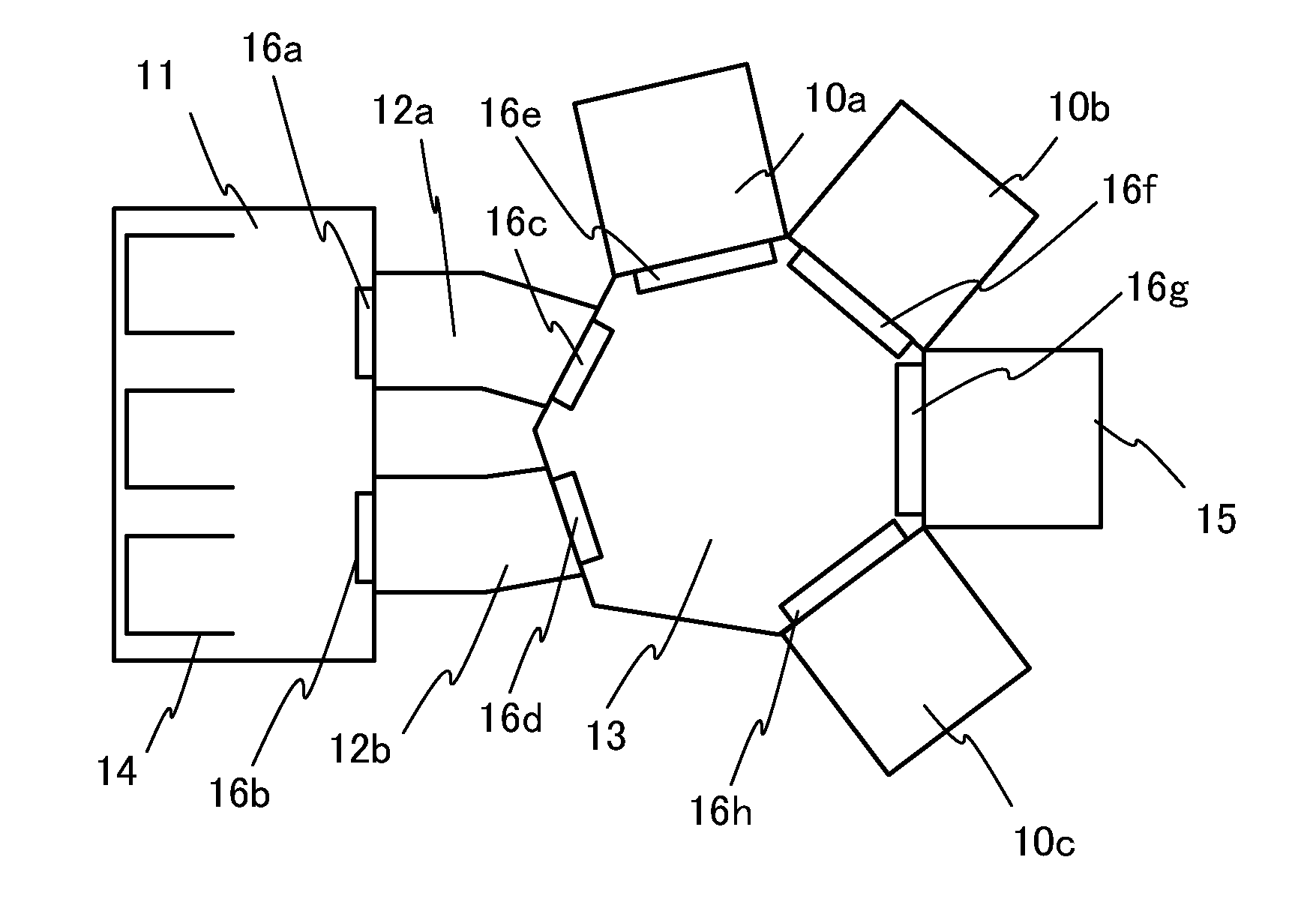
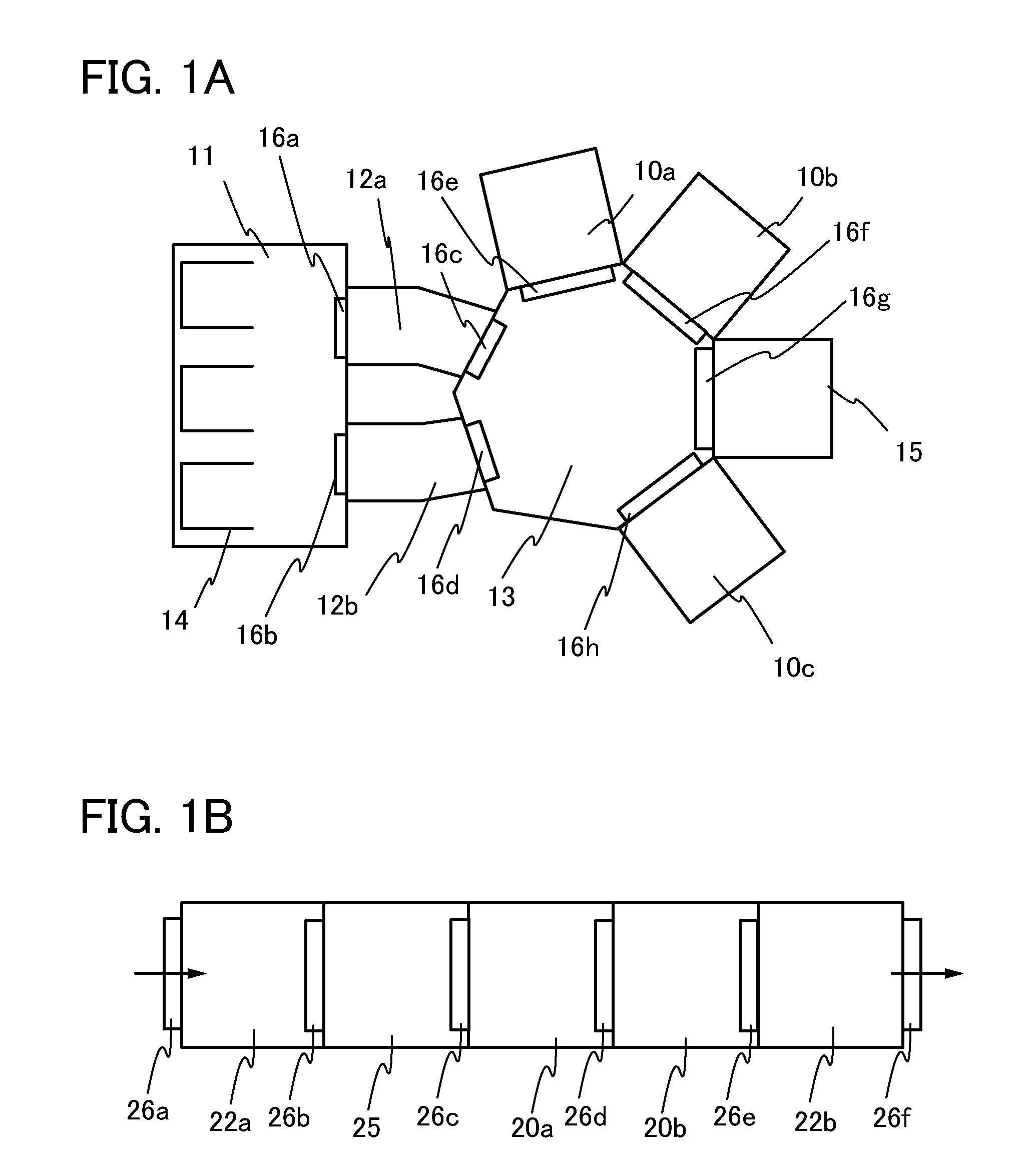
[0041]In this embodiment, a structure of a film formation apparatus with less entry of hydrogen during film formation will be described using FIGS. 1A and 1B.

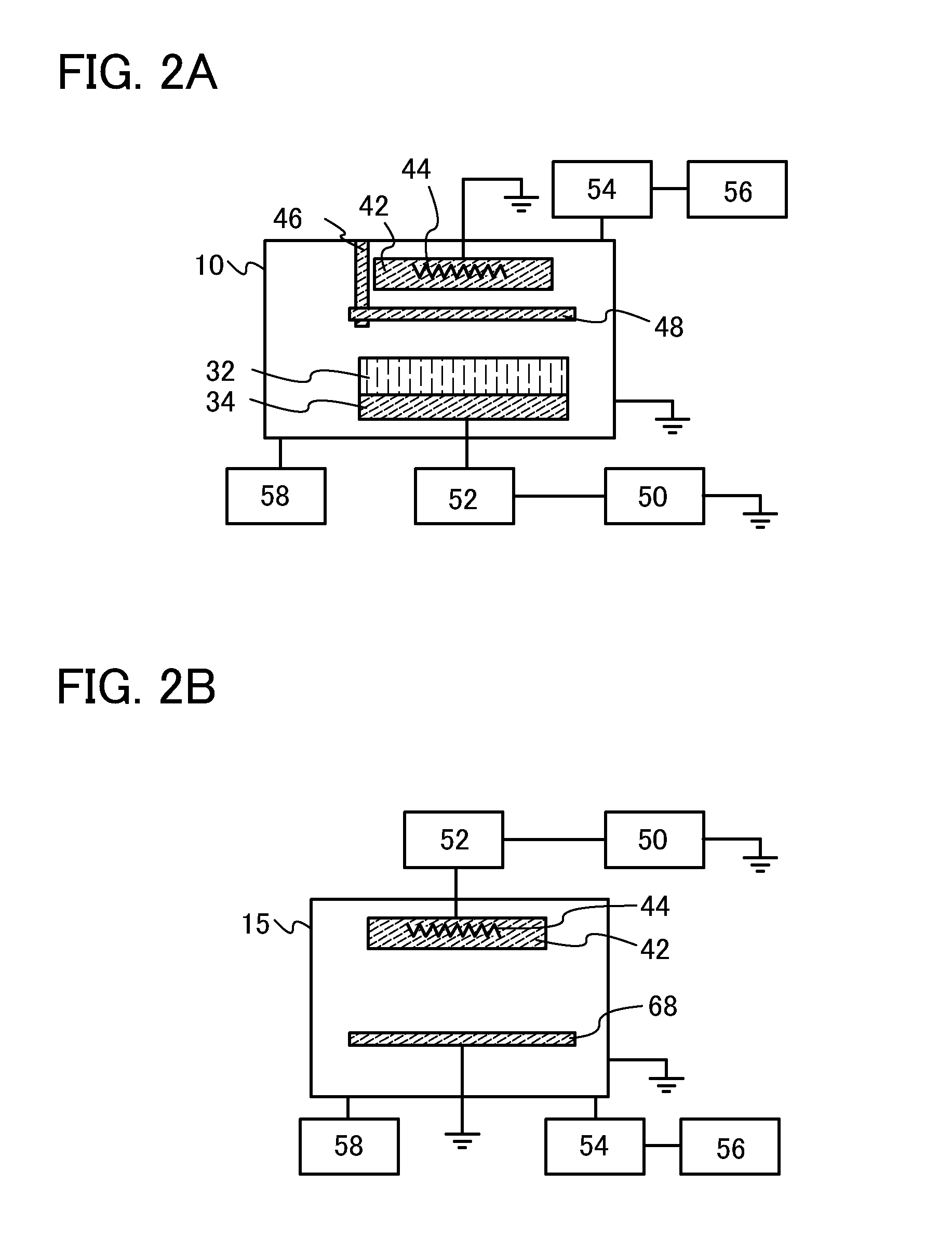
[0042]FIG. 1A illustrates a multi-chamber film formation apparatus. The film formation apparatus includes a substrate supply chamber 11 having three cassette ports 14 accommodating a substrate, a load lock chamber 12a, a load lock chamber 12b, a transfer chamber 13, a substrate heating chamber 15, a film formation chamber 10a with a leakage rate less than or equal to 1×10⁻¹⁰ Pa·m3 / sec, a film formation chamber 10b with a leakage rate less than or equal to 1×10⁻¹⁰ Pa·m3 / sec, and a film formation chamber 10c with a leakage rate less than or equal to 1×10⁻¹⁰ Pa·m3 / sec. The substrate supply chamber is connected to the load lock chamber 12a and the load lock chamber 12b. The load lock chamber 12a and the load lock chamber 12b are connected to the transfer chamber 13. The substrate heating chamber 15 and the film formation chambers 1...

embodiment 2

[0060]In this embodiment, one mode of a method of manufacturing a semiconductor device using a film formation method with less entry of hydrogen will be described with reference to FIGS. 3A to 3C, FIGS. 4A and 4B, FIGS. 5A to 5C, FIGS. 6A to 6E, and FIGS. 7A to 7E.

[0061]In FIGS. 3A to 3C, a top view and cross-sectional views of a transistor 151 which is a top-gate top-contact type is illustrated as an example of a semiconductor device according to one embodiment of the present invention. Here, FIG. 3A is a top view, FIG. 3B is a cross-sectional view along A-B in FIG. 3A, and FIG. 3C is a cross-sectional view along C-D in FIG. 3A. Note that in FIG. 3A, some of the components of the thin film transistor 151 (e.g., a gate insulating film 112) are omitted for brevity.

[0062]The transistor 151 in FIGS. 3A to 3C includes a substrate 100, an insulating film 102 over the substrate 100, an oxide semiconductor film 106 over the insulating film 102, a source electrode 108a and a drain electrode...

embodiment 3

[0139]One mode of a film formation method for an oxide semiconductor film that can be used for a semiconductor film of a transistor in Embodiment 2 will be described using FIGS. 8A to 8C.

[0140]The oxide semiconductor film of this embodiment has a stack structure including a first crystalline oxide semiconductor film and a second crystalline oxide semiconductor film thereover which is thicker than the first crystalline oxide semiconductor film.

[0141]First, the insulating film 102 is formed over the substrate 100.

[0142]Next, a first oxide semiconductor film having a thickness greater than or equal to 1 nm and less than or equal to 10 nm is formed over the insulating film 102. A sputtering method is used for the formation of the first oxide semiconductor film. The substrate temperature during the film formation is greater than or equal to 100° C. and less than or equal to 400° C.

[0143]In this embodiment, the first oxide semiconductor film having a thickness of 5 nm is formed using a ta...


PUM

PropertyMeasurementUnit
distanceaaaaaaaaaa
lengthaaaaaaaaaa
temperatureaaaaaaaaaa

Abstract

There have been cases where transistors using oxide semiconductors are inferior in reliability to transistors using amorphous silicon. There have also been cases where transistors using oxide semiconductors show great variation in electrical characteristics within one substrate, from substrate to substrate, or from lot to lot. Therefore, an object is to manufacture a semiconductor device using an oxide semiconductor which has high reliability and less variation in electrical characteristics. Provided is a film formation apparatus including a load lock chamber, a transfer chamber connected to the load lock chamber through a gate valve, a substrate heating chamber connected to the transfer chamber through a gate valve, and a film formation chamber having a leakage rate less than or equal to 1×10⁻¹⁰ Pa·m3 / sec, which is connected to the transfer chamber through a gate valve.

Description

BACKGROUND OF THE INVENTION[0001]1. Field of the Invention[0002]The present invention relates to a film formation apparatus and a film formation method.[0003]Note that in this specification, a semiconductor device refers to any device that can function by utilizing semiconductor characteristics, and an electro-optical device, a semiconductor circuit, and an electronic device are all semiconductor devices.[0004]2. Description of the Related Art[0005]A technique by which transistors are formed using semiconductor thin films formed over a substrate having an insulating surface has been attracting attention. Such transistors are applied to a wide range of electronic devices, such as integrated circuits (IC) and image display devices (display devices). As materials of semiconductor thin films applicable to the transistors, silicon-based semiconductor materials have been widely used, but oxide semiconductors have been attracting attention as alternative materials.[0006]For example, disclo...

Claims


Application Information

Patent Timeline
Patent Type & Authority Applications(United States)
IPC IPC(8): C23C14/08C23C14/34C23C16/458
CPCC23C14/086C23C14/34C23C14/566H01L29/7869H01L21/67167H01L21/67173H01L21/67207H01L21/02565H01L21/02554C23C14/02C23C14/08C23C14/351C23C14/352C23C14/541
Inventor YAMAZAKI, SHUNPEI
Owner SEMICON ENERGY LAB CO LTD
Why Eureka
Try Eureka