Device switching using layered device structure

a device structure and device technology, applied in semiconductor devices, digital storage, instruments, etc., can solve the problems of increasing power dissipation, preventing proper device operation, and non-scaling of sub-threshold slopes, so as to improve switching and endurance properties, reduce state current, and high defect region

Active Publication Date: 2012-02-23
CROSSBAR INC
View PDF4 Cites 100 Cited by
  • Summary
  • Abstract
  • Description
  • Claims
  • Application Information

AI Technical Summary

Benefits of technology

[0006]The present invention is related to switching devices. More particularly, the present invention provides a structure for a resistive switching memory device. The resistive switching memory device has a reduced on state current for improved switching and endurance properties, among others.
[0007]In a specific embodiment, a switching device structure is provided. The switching device includes a substrate having a surface region and a first dielectric material overlying the surface region. A first electrode overlies the first dielectric material. In a specific embodiment, the first electrode includes at least a metal material. The switching device includes a switching element and a buffer material d...

Problems solved by technology

However, as field effect transistors (FET) approach sizes less than 100 nm, problems such as short channel effect start to prevent proper device operation.
Moreover, such sub 100 nm device size can lead to sub-threshold slope non-scaling and also increases power dissipation.
These devices often require new materials and device structures to couple with silicon based devices to form a memory cell, which lack ...

Method used


Image

  • Device switching using layered device structure
  • Device switching using layered device structure
  • Device switching using layered device structure

Examples


Embodiment Construction

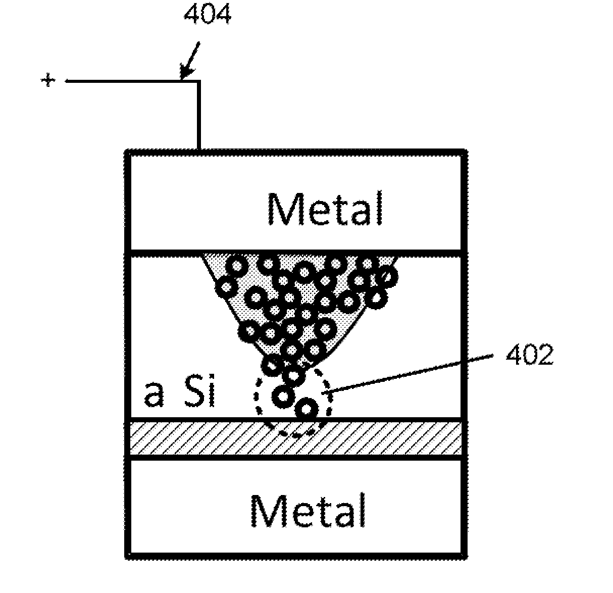
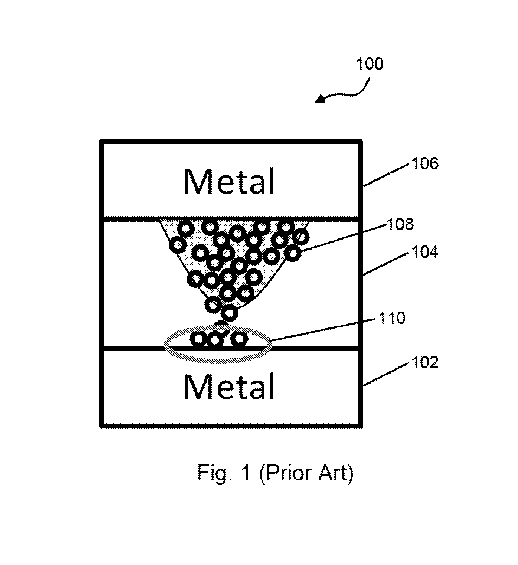
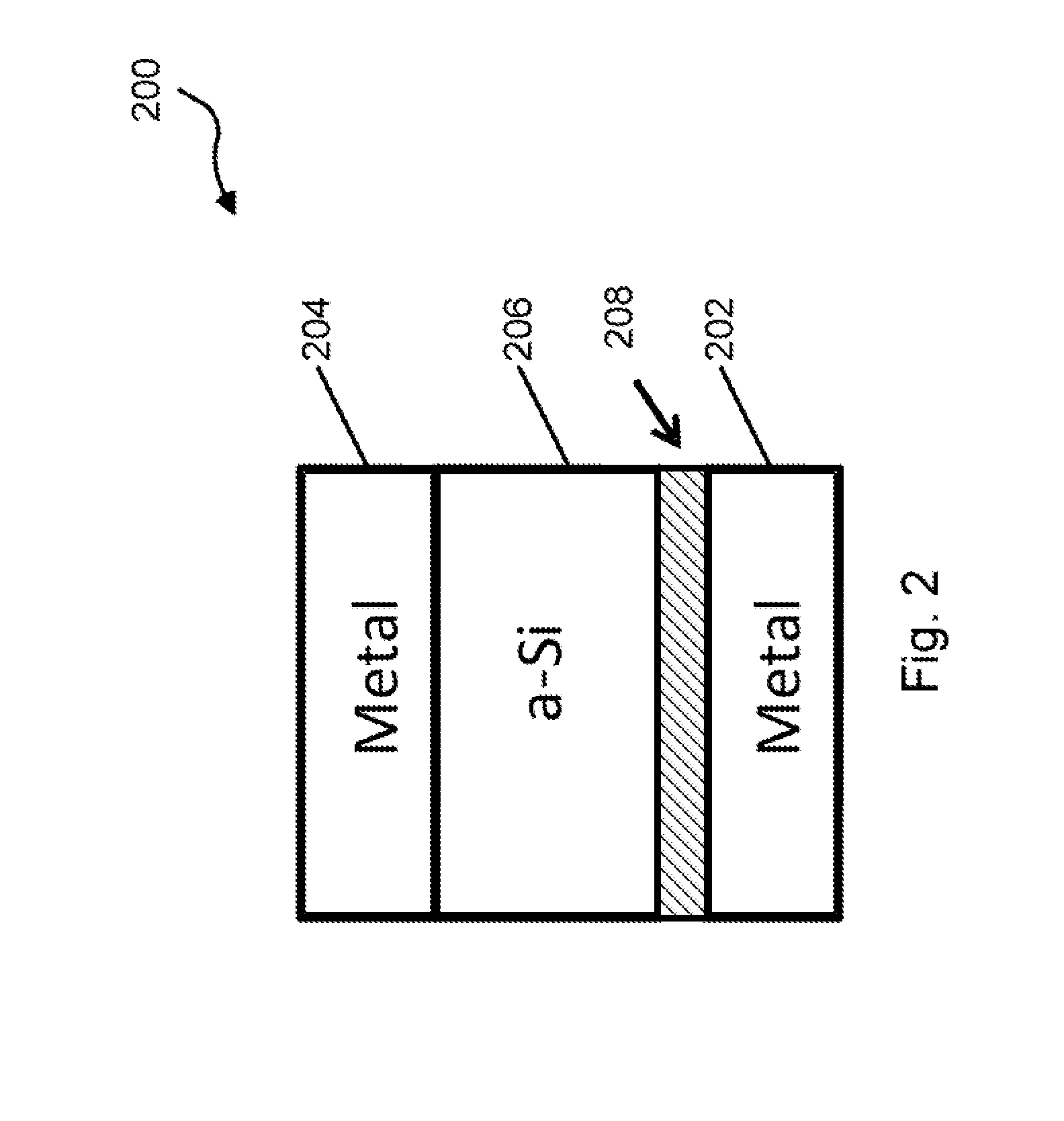
[0016]The present invention is related to switching devices. More particularly, the present invention provides a structure for a resistive switching memory device. The resistive switching memory device is characterized by a reduced on state current for improved switching and endurance properties, among others.

[0017]Resistive switching memory device using a non-crystalline silicon such as amorphous silicon, amorphous-polysilicon and microcrystalline silicon as a switching material and metal electrodes has shown promises in a new class of high density memory devices for fast switching. As merely for illustration, amorphous silicon is used to describe non-crystalline silicon. The on / off behavior of the device depends on metal particles formed in defect sites within the amorphous silicon material. Due to mismatch of materials, defect level in an interface region formed from the amorphous silicon material and a metal electrode is high. As metal particles are formed in the defect sites of...


PUM


Abstract

A resistive switching device. The device includes a first electrode comprising a first metal material overlying the first dielectric material and a switching material comprising an amorphous silicon material. The device includes a second electrode comprising at least a second metal material. In a specific embodiment, the device includes a buffer material disposed between the first electrode and the switching material. The buffer material provides a blocking region between the switching material and the first electrode so that the blocking region is substantially free from metal particles from the second metal material when a first voltage is applied to the second electrode.

Description

CROSS REFERENCE TO RELATED APPLICATIONS[0001]N / ABACKGROUND[0002]The present invention is related to switching devices. More particularly, the present invention provides a structure for a resistive switching memory device. The resistive switching memory device has a reduced on state current to provide improved switching and endurance properties, among others.[0003]The success of semiconductor devices has been mainly driven by an intensive transistor down-scaling process. However, as field effect transistors (FET) approach sizes less than 100 nm, problems such as short channel effect start to prevent proper device operation. Moreover, such sub 100 nm device size can lead to sub-threshold slope non-scaling and also increases power dissipation. It is generally believed that transistor based memories such as those commonly known as Flash may approach an end to scaling within a decade. Flash memory is one type of non-volatile memory device.[0004]Other non-volatile random access memory (RA...

Claims


Application Information

Patent Timeline
IPC IPC(8): H01L45/00
CPCG11C13/0009G11C2213/15G11C2213/33G11C2213/51H01L45/16H01L45/148H01L27/2463H01L45/12H01L45/1233H01L45/085H10N70/245H10N70/801H10N70/826H10N70/884H10N70/011H10N70/20H10B63/30H10B63/80H10N70/021H10N70/841H04L45/12
Inventor JO, SUNG HYUNLU, WEI
Owner CROSSBAR INC
Why Eureka
Try Eureka