Organic Electronic Material, Ink Composition Containing Same, and Organic Thin Film, Organic Electronic Element, Organic Electroluminescent Element, Lighting Device, and Display Device Formed Therewith

a technology of organic electronic elements and ink compositions, which is applied in the direction of conductive materials, solid-state devices, inks, etc., can solve the problems of short element lifetime, low light emission efficiency and short element lifetime, and difficulty in providing a multi-layer structure in polymer-type organic el elements, etc., to achieve superior light emission efficiency, easy formation, and superior emission lifetime

Inactive Publication Date: 2012-03-29
HITACHI CHEM CO LTD
View PDF8 Cites 29 Cited by
  • Summary
  • Abstract
  • Description
  • Claims
  • Application Information

AI Technical Summary

Benefits of technology

[0105]According to the present invention, since a thin film can be stably and easily formed, and the solubility changes through a polymerization reaction, construction of a multilayer structure of organic thin film layers can be easily achieved. Furthermore, since a sufficient change in the solubility can be obtained at low temperature, an organic electronic material that can be applied to a flexible substrate such as a resin substrate, and an ink composition containing the organic electronic material can be provided. Further, according to the present invention, an organic thin film which is formed by using the organic electronic material or the ink composition, an organic electronic element which uses the organic thin film and has superior light emission efficiency and a superior emission lifetime than conventional electronic elements, an organic EL element, a lighting device, and a display device which includes the organic EL element and the lighting device.
[0106]Further, according to the present invention, an organic electronic material which can produce an organic electronic element capable of lowering of the driving voltage or stable long-term driving, and can be cured at low temperature by a coating method, a multilayered organic electronic element using the organic electronic material, an organic electroluminescent element, a display element and a lighting device can be provided. An organic electronic element, particularly an organic EL element, which is capable of lowering of the driving voltage or stable long-term driving can be provided by incorporating an ionic compound and a charge transporting compound.

Problems solved by technology
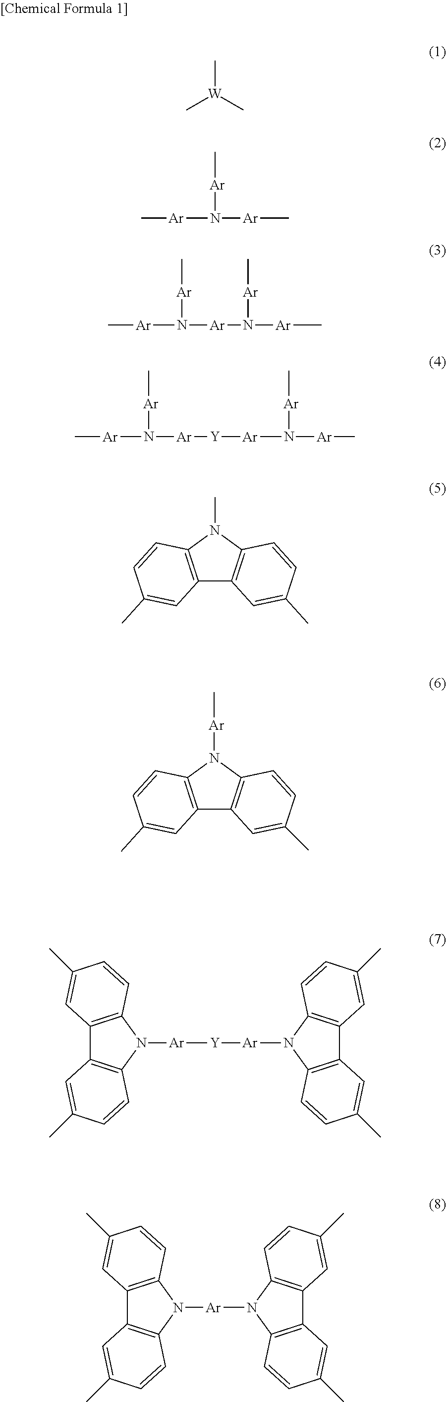
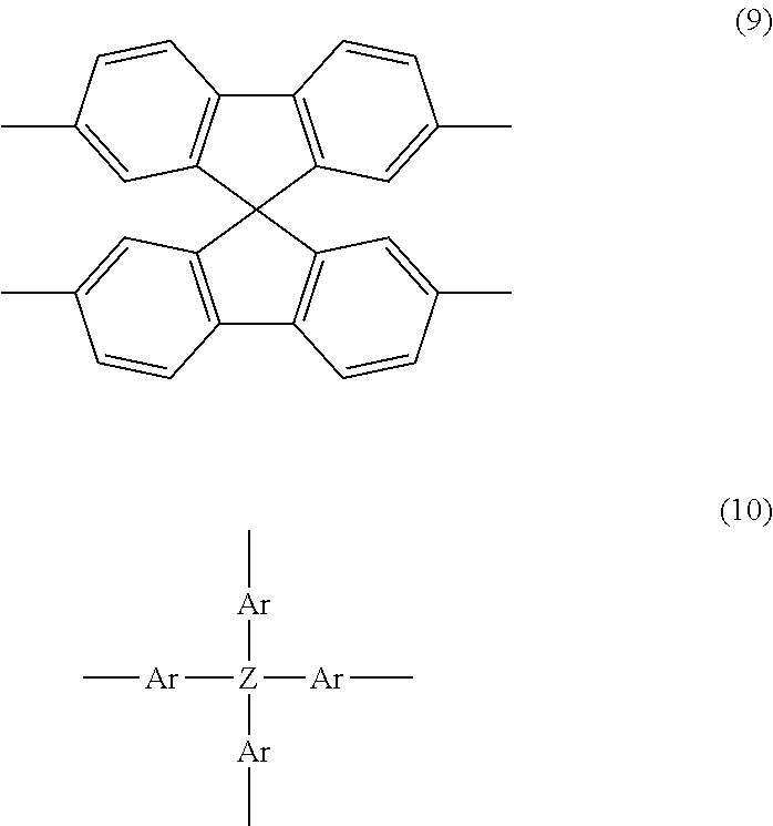
Vigorous research has been conducted so far on the low molecular weight type organic EL elements and the polymer type organic EL elements, but there still are problems of low light emission efficiency and a short element lifetime.
On the other hand, in the case of the polymer type organic EL elements, since film formation is carried out using a wet process such as printing or inkjetting, there occurs a problem that when an upper layer is applied, the lower layer undergoes dissolution.
Therefore, providing a multilayer structure in the polymer type organic EL elements is more difficult than in the case of the low molecular weight type organic EL elements, and the effects of enhancing the light emission efficiency and improving the lifetime could not be obtained.
However, when water-soluble PEDOT:PSS is used, the moisture remaining in the thin film needs to be removed, and this removal of moisture is difficult and causes deterioration of the properties of the organic electronic element.
Further, for the removal of moisture, it is necessary to dry the element at high temperature for a long time period, so that production of an organic electronic element on a resin substrate is difficult, or significant restrictions are imposed on the process, such as reduced pressure conditions.
However, in such a method, the solvent that can be used is limited to a solvent that does not dissolve the lower layer, and therefore, there is a problem that only a narrow choice of materials is available.
Further, a certain degree of erosion occurs in the lower layer at the time of the formation of an upper layer.
However, there is the problem described above that is attributable to the moisture remaining in the thin film when water-soluble PEDOT:PSS is used, or there are problems that there are restrictions on the material that can be used, in order to utilize the difference in solubility, that siloxane compounds are unstable to moisture in air, and that the properties of the element are not satisfactory.
However, since such a substrate undergoes softening, decomposition or degeneration due to high temperature, there is a problem that the method of bringing the polymerization reaction cannot be utilized.
In order to make the compound sufficiently insoluble through this method, there is a problem that ultraviolet irradiation for a long time period is required, and decomposition of triphenylamine or the like occurs.
In these methods, photoinitiators are used, and therefore, there is a concern for deterioration due to light.
Furthermore, there is a problem that sufficient insolubilization at low temperature does not proceed, and, and the application of resin substrates which require low temperature curing is restricted, or there is a problem that at the time of forming an upper layer, the upper layer and the lower layer are intermixed, causing deterioration of the organic EL characteristics.
On the other hand, an investigation is being conducted on the use of an iodonium salt or sulfonium salt having the same structure as that of the photoinitiators in the hole transport layer or the light emitting layer, for the purpose of lowering the driving voltage, which is a problem for organic EL elements.

Method used


Image

  • Organic Electronic Material, Ink Composition Containing Same, and Organic Thin Film, Organic Electronic Element, Organic Electroluminescent Element, Lighting Device, and Display Device Formed Therewith
  • Organic Electronic Material, Ink Composition Containing Same, and Organic Thin Film, Organic Electronic Element, Organic Electroluminescent Element, Lighting Device, and Display Device Formed Therewith
  • Organic Electronic Material, Ink Composition Containing Same, and Organic Thin Film, Organic Electronic Element, Organic Electroluminescent Element, Lighting Device, and Display Device Formed Therewith

Examples


example 1

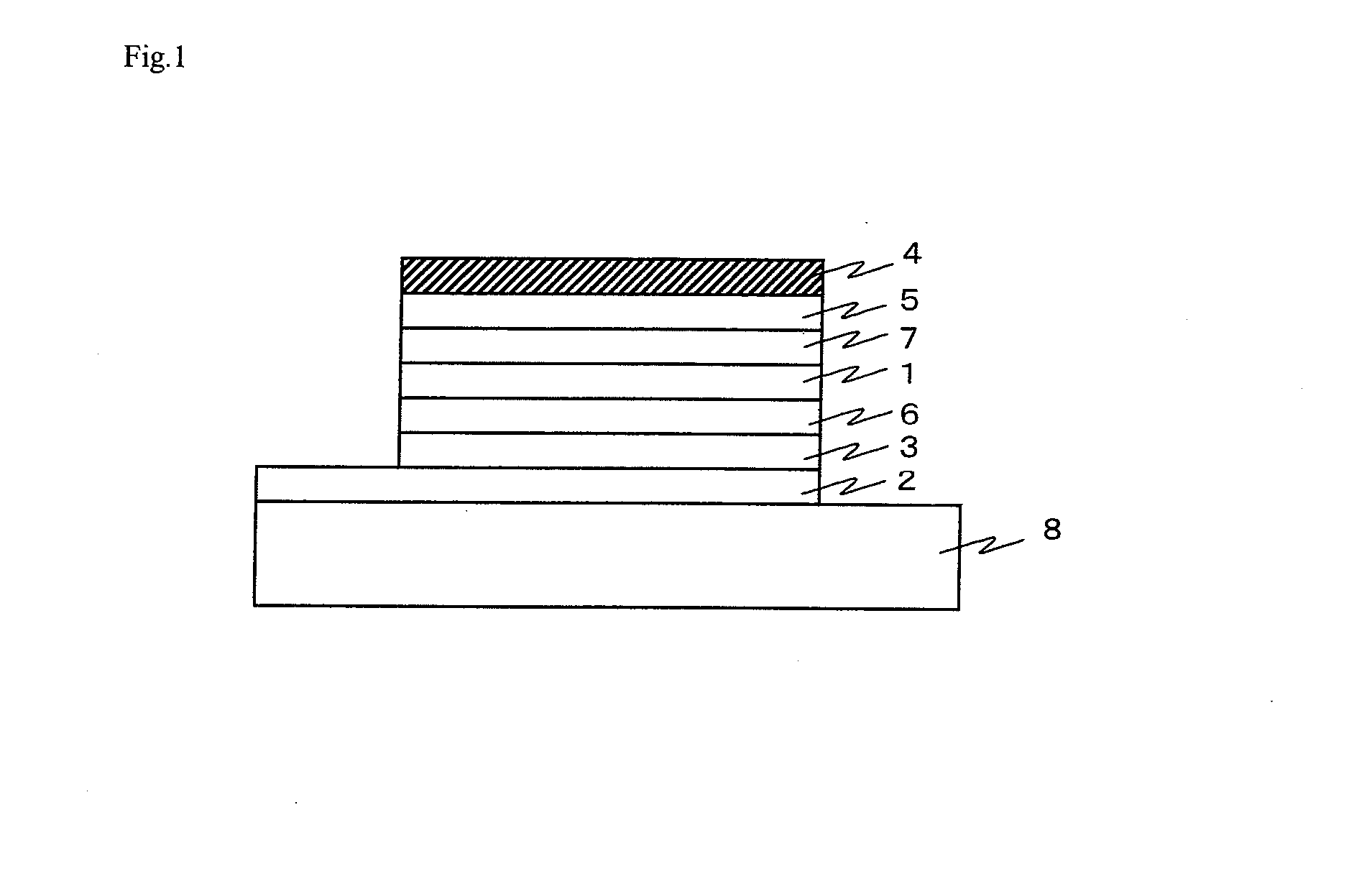
[0297]A PEDOT:PSS dispersion liquid (manufactured by Starck-Vtech, Ltd., A14083 LVW142) was spin coated at 1500 min−1 on a glass substrate having an ITO pattern with a width of 1.6 mm, and the glass substrate was heated to dry on a hot plate at 200° C. for 10 minutes in air. Thus, a hole injection layer (40 nm) was formed. The experiment thereafter was carried out in a dry nitrogen environment.

[0298]Subsequently, a coating solution prepared by mixing the oligomer A (4.5 mg) obtained as described above, a photoinitiator (0.13 mg) which was the ionic compound 1, and toluene (1.2 mL), was spin coated at 3000 min−1 on the hole injection layer, and then the coating solution was irradiated with light (3 J / cm2) using a metal halide lamp. The coating solution was cured by heating on a hot plate at 180° C. for 60 minutes, and thus a hole transport layer (40 nm) was formed.

[0299]Subsequently, the glass substrate thus obtained was transferred into a vacuum deposition apparatus, and CBP+Ir(piq)...

example 2

[0304]

[0305]An element was produced in the same manner as in Example 1, except that a coating solution prepared by mixing the oligomer 13 (4.5 mg) obtained as described above, the initiator (the same as in Example 1) (0.45 mg), and toluene (1.2 mL) was spin coated at 3000 min−1 on the hole injection layer, the coating solution was cured by heating on a hot plate at 120° C. for 10 minutes, and thus a hole transport layer (40 nm) was formed. ITO of this organic EL element was used as the positive electrode, while Al was used as the negative electrode, and a voltage was applied. Red light emission was observed at 4.0 V, and the current efficiency at a luminance of 1000 cd / m2 was 5.0 cd / A. Further, the lifetime characteristics were measured, and the luminance decreased by half in 140 hours.

[0306]

example 3

[0307]A coating solution prepared by mixing the oligomer A (4.5 mg) obtained as described above, the photoinitiator (the same as in Example 1) (0.13 mg), and toluene (500 μL) was spin coated at 3000 min−1 on a glass substrate having an ITO pattern with a width of 1.6 mm. The operation thereafter was carried out in a dry nitrogen environment.

[0308]Subsequently, the coating solution was irradiated with light (3 J / cm2) using a metal halide lamp, and was cured by heating on a hot plate for 15 minutes at 120° C. and for 60 minutes at 180° C. Thus, a hole injection layer (40 nm) was formed.

[0309]Next, sealing was carried out in the same manner as in Example 1, while depositing CBP+Ir(piq)3 (40 nm), BAlq (10 nm), Alq3 (30 nm), LiF (film thickness 0.5 nm), and Al (film thickness 100 nm) in this order.

[0310]ITO of this organic EL element was used as the positive electrode, while Al was used as the negative electrode, and a voltage was applied to the element. Red light emission was observed a...


PUM

PropertyMeasurementUnit
polydispersityaaaaaaaaaa
temperatureaaaaaaaaaa

Abstract

Provided are: an organic electronic material which can be easily multilayered and that can be used in substrates, such as resin, that cannot be processed at high temperatures; an ink composition containing the same; an organic thin film formed using said organic electronic material or said ink composition; and an organic electronic element and an organic EL element that are formed using said organic thin film and that have a superior luminous efficacy and emission lifespan than conventional elements. Specifically, provided are: an organic electronic material that is characterized by containing an oligomer or a polymer having a structure that branches into three or more directions and has at least one polymerizable substituent; an ink composition containing said organic electronic material; and an organic thin film prepared using the aforementioned organic electronic material. Further, provided are an organic electronic element and an organic electroluminescent element containing said organic thin film.

Description

TECHNICAL FIELD[0001]The present invention relates to an organic electronic material and an ink composition containing the material, and an organic thin film, an organic electronic element, an organic electroluminescent element (hereinafter, also referred to as organic EL element), a lighting device and a display device, all of which use the organic electronic material and the ink composition.BACKGROUND ART[0002]Organic electronic elements are elements that carry out an electrical operation using organic substances, and are expected to exhibit features such as energy saving, low price, and flexibility. Thus, more attention is being paid to organic electronic elements as a technology replacing the traditional inorganic semiconductors that are mainly composed of silicon.[0003]Examples of the organic electronic elements include organic EL elements, organic transistors, and organic solar cells.[0004]Among the organic electronic elements, the organic EL elements are attracting attention ...

Claims


Application Information

Patent Timeline
Patent Type & Authority Applications(United States)
IPC IPC(8): H01B1/12C09D11/10C08G73/06C08G73/02C08G73/08
CPCH01L51/0035C09D11/52H01L51/5056H01L51/5088C08G61/12C08G61/124C08G2261/132C08G2261/135C08G2261/1424C08G2261/1644C08G2261/312C08G2261/3162C08G2261/3241C08G2261/411C08G2261/76H01L51/0043H10K85/111H10K85/151H10K50/15H10K50/17C08G73/0266C08G2261/131C08G2261/1434C08G2261/3142C08G2261/354C08G2261/364C08G2261/512C09D165/00C09K11/06C09K2211/1425C09K2211/1433C09K2211/1466H10K71/12H10K85/1135H10K85/115H10K85/113H10K77/111H10K50/11H10K50/82H10K2102/311
Inventor FUNYUU, SHIGEAKIISHITSUKA, KENICHIHOSHI, YOUSUKE
Owner HITACHI CHEM CO LTD
Why Eureka
Try Eureka