Mask blank, transfer mask, method of manufacturing a transfer mask, and method of manufacturing a semiconductor device

a technology of transfer mask and mask, which is applied in the field of mask, transfer mask, method of manufacturing transfer mask, and method of manufacturing semiconductor devices, can solve the problems of large bias (correction amount of pattern line width or the like) due to the electromagnetic field effect, increase the complexity of calculation of this transfer pattern correction, and increase the complexity of the transfer pattern after the correction, so as to reduce the effect of emf bias

Active Publication Date: 2012-04-05
HOYA CORP
View PDF1 Cites 16 Cited by
  • Summary
  • Abstract
  • Description
  • Claims
  • Application Information

AI Technical Summary

Benefits of technology

[0016]First, the present inventors have paid attention to the fact that, in the case of a light-shielding film with a small influence of the EMF effect, it is easy to take advantage of the TMA simulation and thus to reduce the load of EMF bias correction calculation.
[0023]It is an object of this invention to provide a mask blank which comprises a light-shielding film with a reduced EMF bias so that various loads applied to the manufacture of a transfer mask are largely reduced, and which can simultaneously satisfy a condition that when the mask blank is formed into the transfer mask, the light-shielding film ensures an optical density that can prevent sensitization of a resist film on a semiconductor wafer due to leakage light caused by overlapping exposure, and further to provide such a transfer mask, a method of manufacturing such a transfer mask, and a method of manufacturing a semiconductor device using such a transfer mask.
[0072]According to this invention, it is possible to realize and provide a light-shielding film with a reduced EMF bias so that various loads applied to the manufacture of a transfer mask are largely reduced. Further, this light-shielding film with the reduced EMF bias can simultaneously satisfy a condition that the light-shielding film ensures an optical density that can prevent sensitization of a resist film on a semiconductor wafer due to leakage light caused by overlapping exposure.

Problems solved by technology

In the meantime, in binary masks in the DRAM half-pitch (hp) 40 nm and subsequent generations according to the semiconductor device design rule, the line width of a transfer pattern of a transfer mask is smaller than the wavelength 193 nm of ArF exposure light and, as a result of adopting the resolution enhancement technology for coping with it, there has arisen a problem that if the thickness of a light-shielding film pattern in a transfer pattern area (main pattern area) is large, a bias (correction amount of pattern line width or the like) due to the electromagnetic field (EMF) effect becomes large.
Calculation of this transfer pattern correction becomes more complicated as the EMF bias increases.
Further, a transfer pattern after the correction also becomes more complicated as the EMF bias increases.
As a consequence, a large load is applied to the manufacture of the transfer mask.
These new problems have arisen due to the increase in EMF bias.
However, since this is the simulation that does not take into account the EMF effect, the TMA simulation results alone are insufficient for a recent fine pattern which is largely affected by the EMF effect.

Method used


Image

  • Mask blank, transfer mask, method of manufacturing a transfer mask, and method of manufacturing a semiconductor device
  • Mask blank, transfer mask, method of manufacturing a transfer mask, and method of manufacturing a semiconductor device
  • Mask blank, transfer mask, method of manufacturing a transfer mask, and method of manufacturing a semiconductor device

Examples


example 1

[0175](Manufacture of Mask Blank)

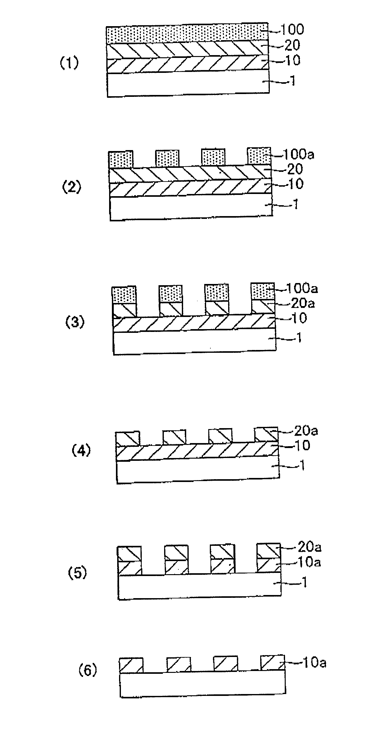
[0176]As shown in FIG. 13, using a synthetic quartz glass substrate having a 6-inch square size with a thickness of 0.25 inches as a transparent substrate 1, a MoSiN film (light-shielding layer 11: lower layer) and a MoSiON film (front-surface antireflection layer 12: upper layer) were formed in this order as a light-shielding film 10 on the transparent substrate 1.

[0177]Specifically, using a mixed target of molybdenum (Mo) and silicon (Si) (Mo:Si=21 at %:79 at %), reactive sputtering (DC sputtering) was carried out in a mixed gas atmosphere of argon (Ar) and nitrogen (N2), thereby forming the light-shielding layer 11 (MoSiN film, N=about 5 at %) to a thickness of 35 nm on the transparent substrate 1.

[0178]Then, using a mixed target of molybdenum (Mo) and silicon (Si) (Mo:Si=4 at %:96 at %), reactive sputtering (DC sputtering) was carried out in a mixed gas atmosphere of argon (Ar), oxygen (O2), and nitrogen (N2), thereby forming the front-surface an...

example 2

[0190](Manufacture of Mask Blank)

[0191]As shown in FIG. 13, using a synthetic quartz glass substrate having a 6-inch square size with a thickness of 0.25 inches as a transparent substrate 1, a MoSi film (light-shielding layer 11: lower layer) and a MoSiON film (front-surface antireflection layer 12: upper layer) were formed in this order as a light-shielding film 10 on the transparent substrate 1.

[0192]Specifically, using a mixed target of molybdenum (Mo) and silicon (Si) (Mo:Si=9.5 at %:89.5 at %), sputtering (DC sputtering) was carried out in an argon (Ar) gas atmosphere, thereby forming the light-shielding layer 11 (MoSi film) to a thickness of 38 nm on the transparent substrate 1.

[0193]Then, using a mixed target of molybdenum (Mo) and silicon (Si) (Mo:Si=4 at %:96 at %), reactive sputtering (DC sputtering) was carried out in a mixed gas atmosphere of argon (Ar), oxygen (O2), and nitrogen (N2), thereby forming the front-surface antireflection layer 12 (MoSiON film) to a thickness...

example 3

[0205](Manufacture of Mask Blank)

[0206]As shown in FIG. 13, using a synthetic quartz glass substrate having a 6-inch square size with a thickness of 0.25 inches as a transparent substrate 1, a MoSi film (light-shielding layer 11: lower layer) and a MoSiON film (front-surface antireflection layer 12: upper layer) were formed in this order as a light-shielding film 10 on the transparent substrate 1.

[0207]Specifically, using a mixed target of molybdenum (Mo) and silicon (Si) (Mo:Si=9.5 at %:89.5 at %), sputtering (DC sputtering) was carried out in an argon (Ar) gas atmosphere, thereby forming the light-shielding layer 11 (MoSi film) to a thickness of 39 nm on the transparent substrate 1.

[0208]Then, using a mixed target of molybdenum (Mo) and silicon (Si) (Mo:Si=4 at %:96 at %), reactive sputtering (DC sputtering) was carried out in a mixed gas atmosphere of argon (Ar), oxygen (O2), and nitrogen (N2), thereby forming the front-surface antireflection layer 12 (MoSiON film) to a thickness...


PUM

PropertyMeasurementUnit
thicknessaaaaaaaaaa
optical densityaaaaaaaaaa
thicknessaaaaaaaaaa

Abstract

A mask blank for use in the manufacture of a binary mask adapted to be applied with ArF excimer laser exposure light has, on a transparent substrate, a light-shielding film for forming a transfer pattern. The light-shielding film has a laminated structure of a lower layer and an upper layer and has an optical density of 2.8 or more for exposure light and a thickness of 45 nm or less. The lower layer is made of a material in which the total content of a transition metal and silicon is 90 at % or more, and has a thickness of 30 nm or more. The upper layer has a thickness of 3 nm or more and 6 nm or less. The phase difference between exposure light transmitted through the light-shielding film and exposure light transmitted in air for a distance equal to the thickness of the light-shielding film is 30 degrees or less.

Description

[0001]This application is based upon and claims the benefit of priority from Japanese Patent Application No. 2010-221661, filed on Sep. 30, 2010, the disclosure of which is incorporated herein in its entirety by reference.TECHNICAL FIELD[0002]This invention relates to a mask blank and a transfer mask for use in the manufacture of semiconductor devices or the like and further relates to a method of manufacturing a transfer mask and a method of manufacturing a semiconductor device.BACKGROUND ART[0003]The miniaturization of semiconductor devices and the like is advantageous in bringing about an improvement in performance and function (higher-speed operation, lower power consumption, etc.) and a reduction in cost and thus has been accelerated more and more. The lithography technique has been supporting this miniaturization and transfer masks are a key technique along with exposure apparatuses and resist materials.[0004]In recent years, the development of the DRAM half-pitch (hp) 45 nm t...

Claims


Application Information

Patent Timeline
Patent Type & Authority Applications(United States)
IPC IPC(8): H01L21/268G03F1/50G03F1/48G03F7/20
CPCG03F1/58H01L21/266G03F7/20G03F1/00G03F1/50H01L21/268G03F1/46H01L21/0276G03F1/66H01L21/0337G03F1/26G03F7/2041H01L21/31138
Inventor KOMINATO, ATSUSHIHASHIMOTO, MASAHIRONOZAWA, OSAMU
Owner HOYA CORP
Why Eureka
Try Eureka