Method of manufacturing a multitude of micro-optoelectronic devices, and micro-optoelectronic device
- Summary
- Abstract
- Description
- Claims
- Application Information
AI Technical Summary
Benefits of technology
Problems solved by technology
Method used
Image

Examples
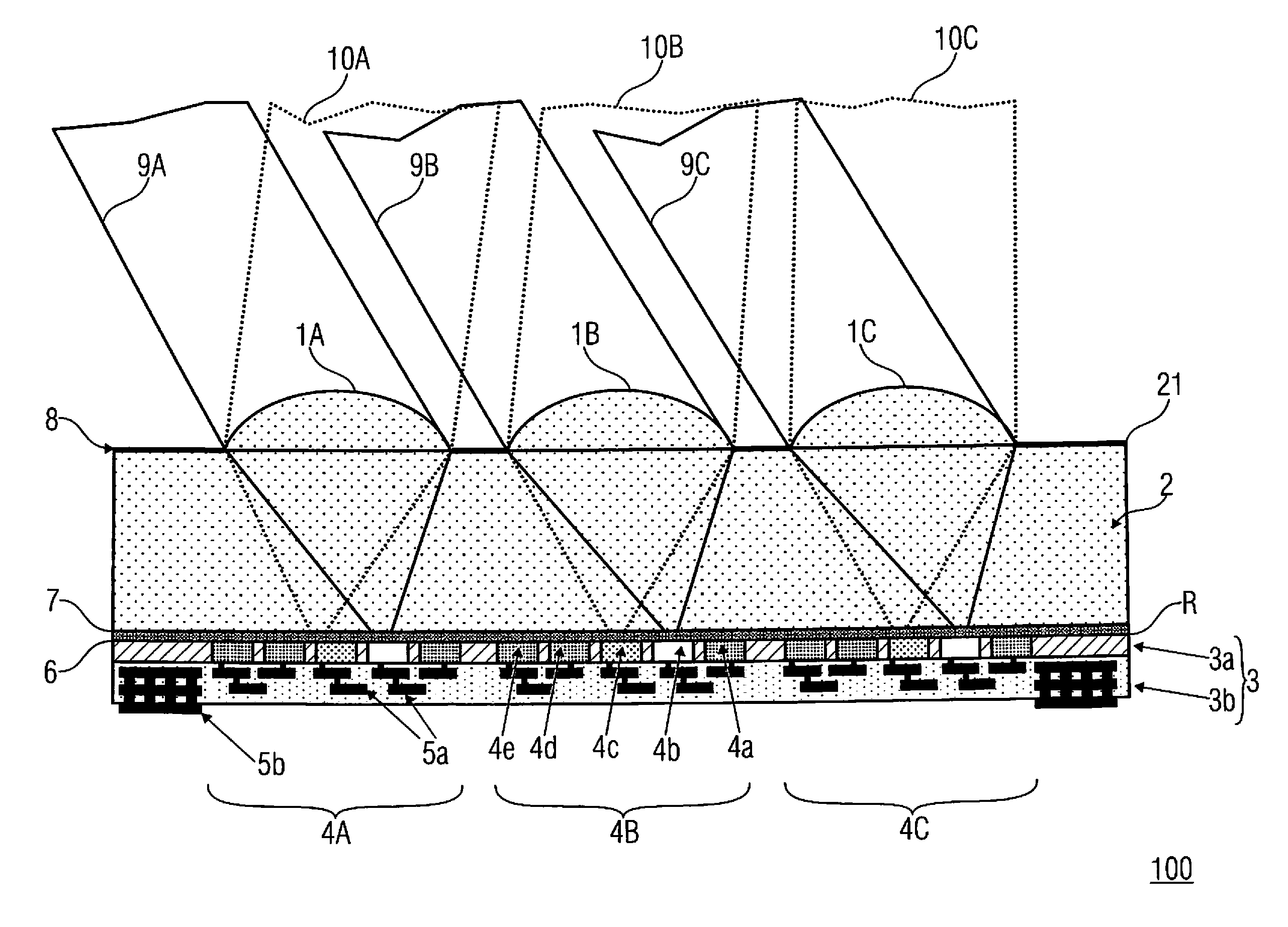
embodiment 100
[0094]FIG. 3A shows a cross-section of a further embodiment of a wafer stack section 300 comprising an image sensor wafer 3 for rear-side exposure, as is described in FIG. 1A, said wafer stack section 300 comprising—in contrast to the embodiment 100 in FIG. 1A—no lens structures 1A to 1C on the surface associated with the incidence of light 15a-15c, however, but having concave micro-optical elements 1A′-1C′ on the side associated with the image sensor wafer 3. A further wafer or wafer section 13 having cavities 13A-13C, which may also be referred to as through-openings, is arranged between the image sensor wafer 3 and the glass wafer 2. In the additional wafer piece 13, the cavities 13A-13C are arranged above the corresponding light sensor arrangements 4A-4C, so that light is refracted by the concave micro-optical structures 1A'-1C′ and impinges on the light sensor arrangements 4A-4C through the cavities 13A-13C.
[0095]FIG. 3A shows three pencils of light 15a-15c which impinge upon t...
embodiment 400
[0106]FIG. 4A shows a further embodiment 400 of a wafer stack section which is very similar to that of FIG. 3A but wherein the cavities 13A-13C were etched directly into the substrate of the sensor wafer 3 or, to be more precise, into the substrate of the semiconductor portion 3a (which may also be referred to as the substrate portion 3a), in contrast to the wafer stack section of FIG. 3A. To emphasize this structural difference as compared to FIG. 3A, the semiconductor material portion 3a is designated here by 3a′, the image sensor wafer is designated by 3′, and the joining zone between the image sensor wafer 3′ and the glass wafer 2 is designated by 12′ (silicon wafer 3′ with cavities worked into it, 12′: joining zone between the silicon wafer 3′ and the glass wafer 2, may also contain an oxide layer; pencil of rays 15a-15c with an auxiliary focal line, see dashed line).
[0107]Production of such embodiments entails very homogeneous control of the etching depth. In embodiments of th...
embodiment 500
[0112]FIG. 5A shows a further embodiment 500 of a wafer section wherein the sensor wafer 3″, more specifically the semiconductor portion 3a″, forms the basic material from which the micro-optics structures 1A-1C are formed, e.g. by a rear-side etch attack, a lithographically produced structure or local material changes such as doping, diffusion or oxidation. In other words, the image sensor wafer 3″ itself is optically structured. Therefore, embodiments 500 may also be referred to as micro-optoelectronic devices or wafer sections for short, wherein the micro-optics 1A-1C is an integral constituent of the sensor wafer 3″. Here, the first layer 3a″ is a silicon substrate, for example, which is transparent in the infrared range. Thus, the semiconductor material itself may be used for refractive optics or may serve as a substrate for optics elements. From that point of view, it is sufficient, with such embodiments that are to be operated in infrared light, for only their rear sides R to...
PUM
 Abstract
Description
Claims
Application Information
PatSnap Eureka turns technology decisions into work you can execute. Powered by our Innovation Knowledge Graph, it runs expert workflows across engineering, life sciences, materials and intellectual property. Get your review-ready output in minutes.


