Semiconductor device and method for manufacturing the same

a semiconductor device and semiconductor technology, applied in the direction of semiconductor devices, electrical devices, transistors, etc., can solve the problems of increasing the carrier density, increasing the takt time for manufacturing, and difficult to obtain an oxide semiconductor layer whose on characteristics are suitable for a desired semiconductor device, etc., to achieve sufficient characteristics and favorable contact characteristics

Active Publication Date: 2012-05-10
SEMICON ENERGY LAB CO LTD
View PDF17 Cites 21 Cited by
  • Summary
  • Abstract
  • Description
  • Claims
  • Application Information

AI Technical Summary

Benefits of technology

[0019]In addition, according to one embodiment of the present invention, a semiconductor device including an oxynitride semiconductor whose carrier density is controlled can be manufactured, and sufficient on characteristics can be obtained even without heat treatment. Further, even when a low resistance layer or the like is not provided between a semiconductor layer and a source electrode and between the semiconductor layer and a drain electrode, favorable contact characteristics can be exhibited.

Problems solved by technology

However, an increase of the carrier density is difficult to control by heat treatment, and it is difficult to obtain an oxide semiconductor layer whose on characteristics are suitable for a desired semiconductor device.
In addition, in the case where a large-sized or a large-area semiconductor device using an oxide semiconductor is intended, performing heat treatment is not favorable because it causes an increase of the takt time for manufacturing and an increase of the cost.

Method used


Image

  • Semiconductor device and method for manufacturing the same
  • Semiconductor device and method for manufacturing the same
  • Semiconductor device and method for manufacturing the same

Examples


embodiment 1

[0038]In this embodiment, modes of a semiconductor device and a method for manufacturing the semiconductor device will be described with reference to FIGS. 1A to 1C, FIGS. 2A to 2D, FIGS. 3A to 3E, FIGS. 4A to 4E, FIGS. 5A to 5E, FIGS. 6A to 6E, FIGS. 7A to 7E, and FIG. 15.

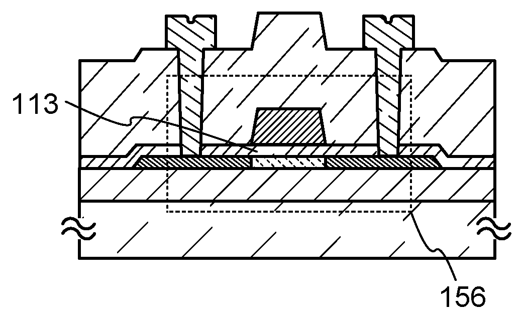
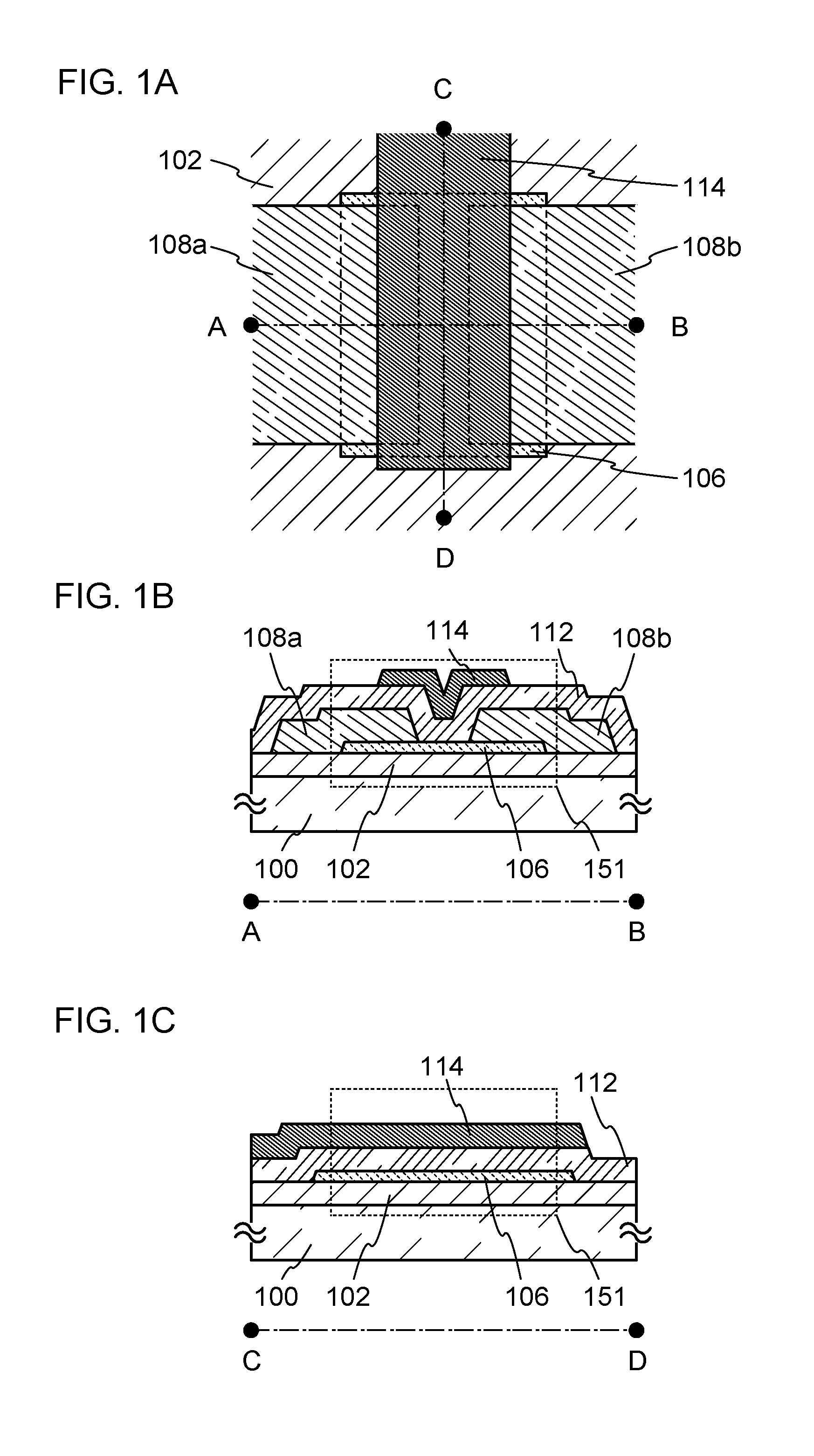
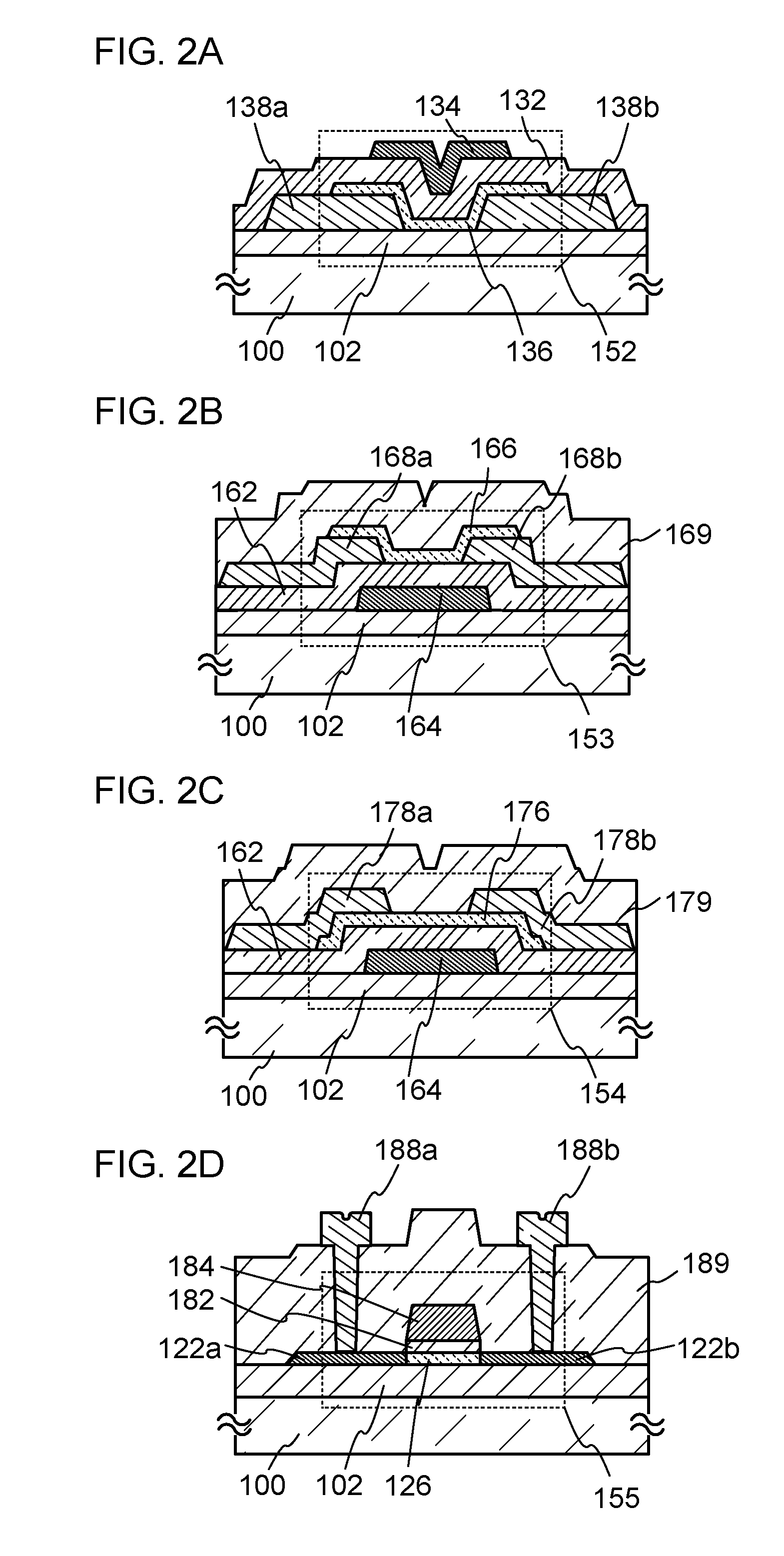
[0039]FIGS. 1A to 1C are a plan view and cross-sectional views, illustrating a transistor 151 which is a top-gate top-contact transistor as an example of a semiconductor device of an embodiment of the present invention. Here, FIG. 1A is a plan view, FIG. 1B is a cross-sectional view along A-B of FIG. 1A, and FIG. 1C is a cross-sectional view along C-D of FIG. 1A. Note that some components of the transistor 151 (e.g., a gate insulating layer 112) are omitted in FIG. 1A for brevity.

[0040]The transistor 151 illustrated in FIGS. 1A to 1C includes, over a substrate 100, a base insulating layer 102, an oxide semiconductor layer 106, a source electrode 108a, a drain electrode 108b, the gate insulating layer 112, and a ga...

embodiment 2

[0127]A semiconductor device having a display function (also referred to as a display device) can be manufactured with the use of the transistor exemplified in Embodiment 1. Moreover, part or all of driver circuitry which includes the transistor can be formed over a substrate where a pixel portion is formed, whereby a system-on-panel can be obtained.

[0128]In FIG. 8A, a sealant 205 is provided so as to surround a pixel portion 202 provided over a first substrate 201, and the pixel portion 202 is sealed between the first substrate 201 and a second substrate 206. In FIG. 8A, a scan line driver circuit 204 and a signal line driver circuit 203 which are formed using a single crystal semiconductor layer or a polycrystalline semiconductor layer over a substrate separately prepared are mounted in a region that is different from the region surrounded by the sealant 205 over the first substrate 201. Further, various signals and potentials are supplied to the signal line driver circuit 203 and...

embodiment 3

[0183]A semiconductor device which is an embodiment of the present invention can be applied to a variety of electronic appliances (including game machines). Examples of electronic appliances include a television set (also referred to as a television or a television receiver), a monitor of a computer or the like, a camera such as a digital camera or a digital video camera, a digital photo frame, a mobile phone set (also referred to as a mobile phone or a mobile phone device), a portable game console, a portable information terminal, an audio reproducing device, a large-sized game machine such as a pachinko machine, and the like. Examples of electronic appliances each including the semiconductor device described in the above embodiment will be described.

[0184]FIG. 12A illustrates an example of a notebook personal computer including a main body 301, a housing 302, a display portion 303, a keyboard 304, and the like. By applying the semiconductor device described in Embodiment 1 or 2, t...


PUM


Abstract

An object is to provide a semiconductor device including an oxynitride semiconductor whose carrier density is controlled. By introducing controlled nitrogen into an oxide semiconductor layer, a transistor in which an oxynitride semiconductor having desired carrier density and on characteristics is used for a channel can be manufactured. Further, with the use of the oxynitride semiconductor, even when a low resistance layer or the like is not provided between an oxynitride semiconductor layer and a source electrode and between the oxynitride semiconductor layer and a drain electrode, favorable contact characteristics can be exhibited.

Description

BACKGROUND OF THE INVENTION[0001]1. Field of the Invention[0002]The present invention relates to a semiconductor device and a method for manufacturing the semiconductor device.[0003]Note that the semiconductor device in this specification refers to all devices that can function by utilizing semiconductor characteristics, and electro-optic devices, semiconductor circuits, and electronic appliances are all semiconductor devices.[0004]2. Description of the Related Art[0005]Transistors formed over a glass substrate or the like are typically manufactured using amorphous silicon, polycrystalline silicon, or the like, as typically seen in liquid crystal display devices. Although transistors including amorphous silicon have low field-effect mobility, they can be formed over a larger glass substrate. On the other hand, although transistors including polycrystalline silicon have high field-effect mobility, they are not suitable for being formed over a larger glass substrate.[0006]In contrast ...

Claims


Application Information

Patent Timeline
Patent Type & Authority Applications(United States)
IPC IPC(8): H01L29/786H01L21/44
CPCH01L29/7869H01L27/1225H01L21/02565H01L29/66742H01L21/02631H01L21/02664H01L21/441H01L21/465H01L29/24H01L29/66969
Inventor ENDO, YUTASASAKI, TOSHINARINODA, KOSEI
Owner SEMICON ENERGY LAB CO LTD
Why Eureka
Try Eureka