Cu-Al ALLOY POWDER, ALLOY PASTE UTILIZING SAME, AND ELECTRONIC COMPONENT
- Summary
- Abstract
- Description
- Claims
- Application Information
AI Technical Summary
Benefits of technology
Problems solved by technology
Method used
Image
Examples
example 1
[0051]This example illustrates an embodiment of the control of the grain size distribution of a Cu—Al alloy powder, which control is important for cost reduction in method for manufacturing forming an electrode, a wiring, and / or a contact member of an electronic component. Specifically, a yield of 90% or more with respect to materials charged in the alloymelting step could be attained according to the present invention in the method for manufacturing a Cu—Al alloy powder including the steps of melting a Cu—Al alloy; powdering the molten alloy by spraying from a nozzle; drying the powder; classifying the dried powder; blending the classified powder; and deoxidizing / dehydrating the powder. This was achieved by controlling the maximum of particle size in particle size distribution of the Cu—Al alloy powder (spherical) to a diameter of 30 μm or less and controlling the average particle size of the alloy powder to 5 μm or less. An exemplary particle size distribution of the Cu—Al alloy p...
example 2
[0054]This example illustrates exemplary classifying processes for the control of particle size distribution of a Cu—Al alloy powder in the manufacturing method of the Cu—Al alloy powder according to the present invention. The manufacturing method includes the steps of melting a Cu—Al alloy; powdering the molten alloy by spraying from a nozzle; drying the powder; classifying the dried powder; blending the classified powder; and deoxidizing / dehydrating the powder. Initially, an exemplary classification through low-cost spontaneous precipitation will be illustrated below as an example of wet classification. Initially, Cu—Al alloy powder particles (Al: 8 percent by weight, density: 8.4 g / cm3) according to the present invention were prepared by water atomization. The water atomization includes the steps of melting a Cu—Al alloy for use in the present invention; powdering the molten alloy by spraying from a nozzle; drying the powder; classifying the dried powder; blending the classified ...
example 3
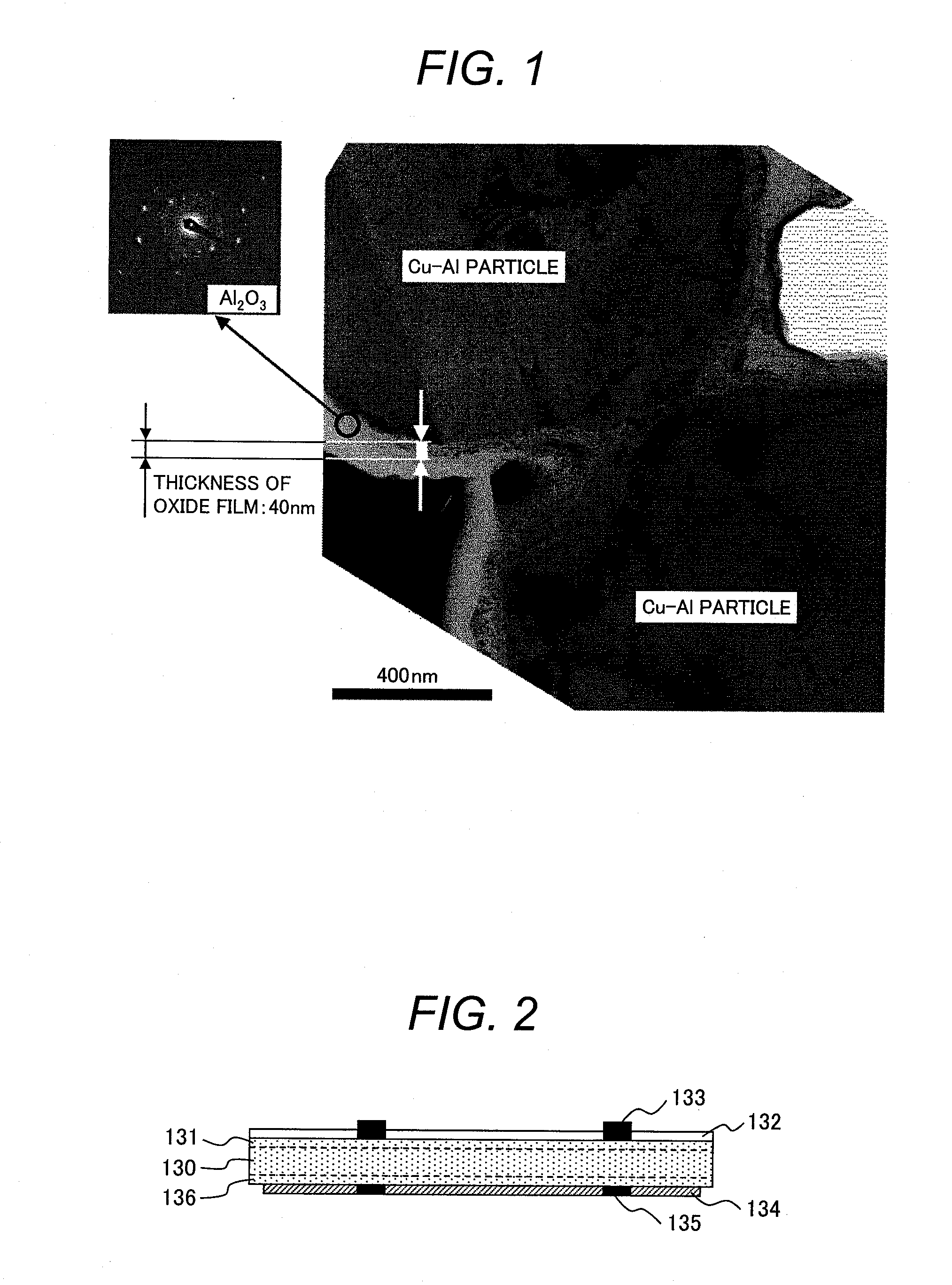
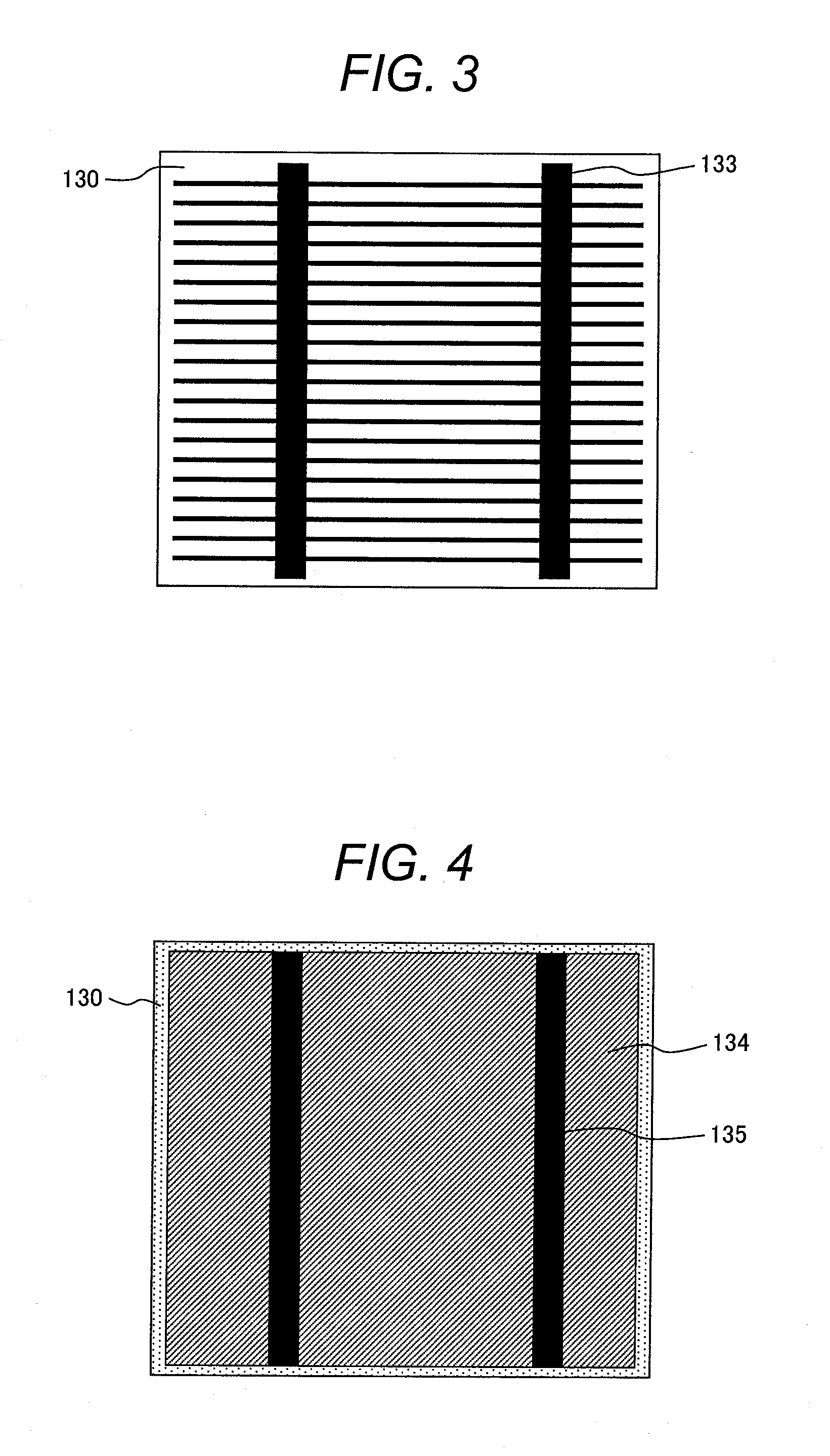
[0056]An embodiment in which an electrode according to the present invention is adopted to a double-sided electrode crystalline silicon (Si) solar cell element according to the present invention will be described. FIGS. 2, 3, and 4 schematically illustrates a cross section, a light-receiving surface, and a back surface, respectively, of the solar cell element.
[0057]A semiconductor substrate 130 of the solar cell element generally employs, for example, monocrystalline or polycrystalline silicon. The semiconductor substrate 130 contains, for example, boron to serve as a p-type semiconductor. The light-receiving surface has depressions and protrusions formed through etching so as to suppress the reflection of sunlight. The light-receiving surface is doped typically with phosphorus to form an n-type semiconductor diffusion layer 131 having a thickness on the order of submicron, and a p-n junction is formed at the interface with the p-type bulk. In addition, an antireflection layer 132 t...
PUM
| Property | Measurement | Unit |
|---|---|---|
| Percent by mass | aaaaa | aaaaa |
| Thickness | aaaaa | aaaaa |
| Percent by mass | aaaaa | aaaaa |
Abstract
Description
Claims
Application Information


