Semiconductor device and method of manufacturing the same

a technology of semiconductor devices and semiconductors, applied in the field of semiconductor devices, can solve the problems of deteriorating the performance of proportionally scaled devices, affecting the efficiency of the device, and affecting the performance of the proportionally scaled device, so as to improve the immunity of short channel effects, reduce the schottky barrier height (sbh), and improve the thermal stability

Inactive Publication Date: 2012-06-07
INST OF MICROELECTRONICS CHINESE ACAD OF SCI
View PDF7 Cites 27 Cited by
  • Summary
  • Abstract
  • Description
  • Claims
  • Application Information

AI Technical Summary

Benefits of technology

[0026]These MOSFETs with epitaxially grown ultrathin metal silicide source / drain characterized by dopant segregation at the interfaces between silicide source / drain and channel region have many advantages. First, by replacing traditional highly doped source / drain with metal silicide source / drain, the ever-deteriorating problem of parasitic series resistance and contact resistance can be alleviated to a great extent, which can greatly improve the short channel effects immunity in the sub-20 nm CMOS technology nodes. Second, because the metal silicide precursor may be well controlled (namely, the thickness of the deposited metal layer and the processing parameters, particularly the time and the temperature range for the first annealing may be well controlled), the formed epitaxially grown ultrathin silicide film is made to have a better thermal stability and subjected to the silicide as diffusion source method to reduce the Schottky Barrier Height (SBH). Specifically, dopant segregation is formed at the silicide / silicon interface between each of the epitaxially grown ultrathin silicide source / drain and the channel region, thereby reducing the SBH and enhancing the driving capability of the device. Moreover, the second annealing under a high temperature for lowering the SBH may repair the damage of the silicide film caused by ion implantation. In short, by employing the MOSFET and the method for manufacturing the same according to embodiments of the present invention, MOSFETs with thermally stable epitaxially grown ultrathin metal silicide source / drain may be obtained in combination with the SADS method to reduce the SBH thus improving the driving capability of such devices.

Problems solved by technology

Although scaling the device size results in a greater process fluctuation, many physical parameters, such as the silicon forbidden band, the Fermi potential, interface states, oxide layer charges, thermoelectric potentials, and p-n junction built-in potentials, cannot be scaled proportionally.
These will greatly deteriorate the performance of proportionally scaled device.
One problem resulting in deterioration is the source / drain series resistance.
However, the source / drain resistance is not proportionally scaled with the scaling of size.
In particular, the contact resistance increases approximately in an inverse square relationship with the scaling down of the size, which causes drops of equivalent operating voltages.
However, with the reduction of the metal silicide source / drain thickness, its thermal stability will also be deteriorated.
However, the thinned silicide films 30 / 31 inherently suffer from poor thermal stability during annealing, for example easy segregation, thus leading to drastically sheet resistance increase.
As a result, the SBH cannot be decreased for the MOSFET with thin metal silicide source / drain.
However, in the sub-20 nm technology nodes, the existing SADS method to improve the driving capability through decreasing the SBH between the silicide source and the channel region cannot be implemented, because thin metallic silicide source / drain cannot bear the high-temperature annealing

Method used


Image

  • Semiconductor device and method of manufacturing the same
  • Semiconductor device and method of manufacturing the same
  • Semiconductor device and method of manufacturing the same

Examples


Embodiment Construction

[0033]Hereinafter, features and technical merits of various technical solutions of the present invention will be described in detail with reference to the drawings and in conjunction with illustrative embodiments. The present invention discloses a MOSFET with epitaxially grown ultrathin metal silicide source / drain that shows excellent thermal stability and a method for manufacturing the same. It should be noted that like numerals indicate like structures. In this application, the phrases “first,”“second,”“over,” and “beneath” may be used to modify various device structures. These modifications, otherwise specifically indicated, do not imply the spatial, sequential or hierarchical relationship of the modified device structure.

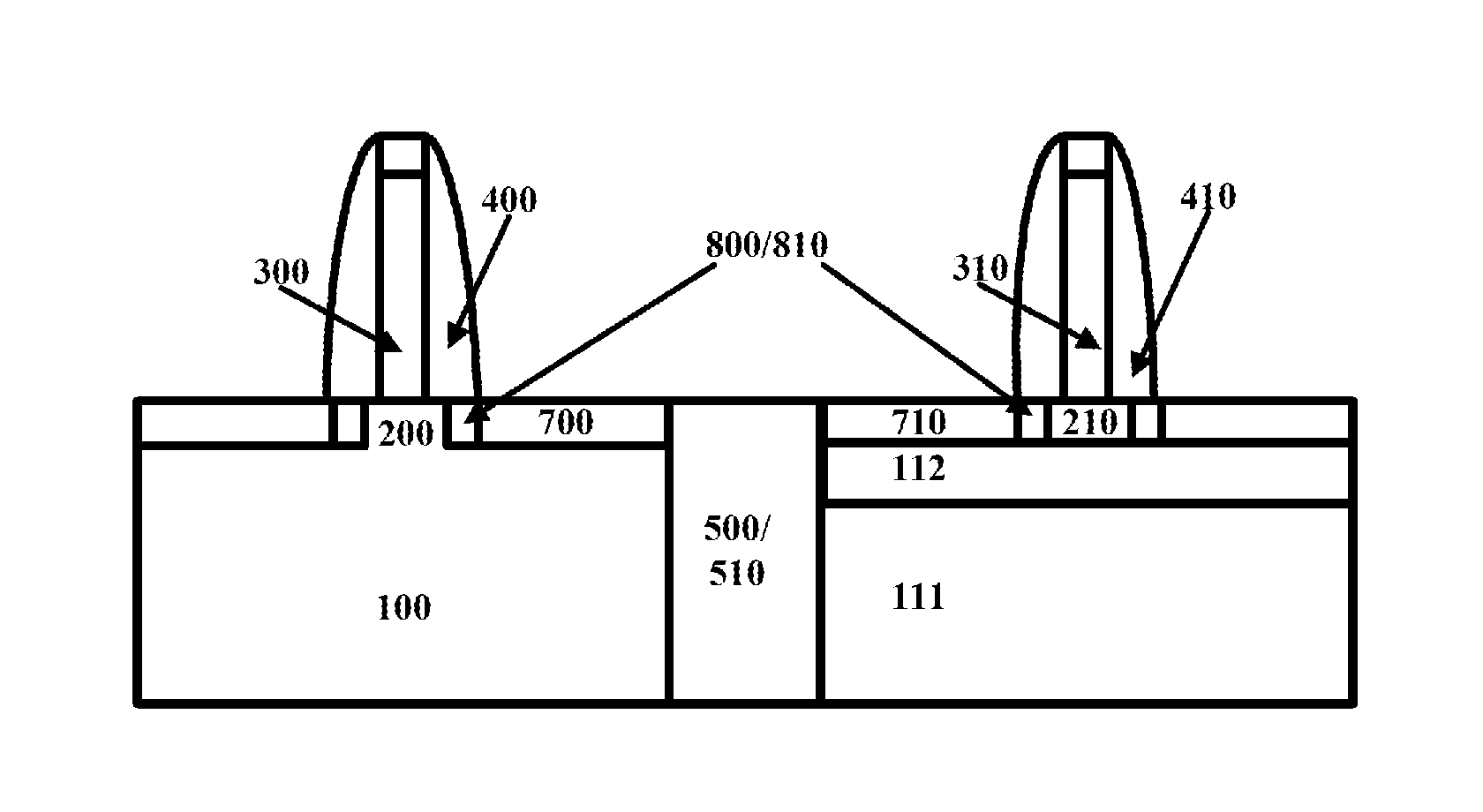
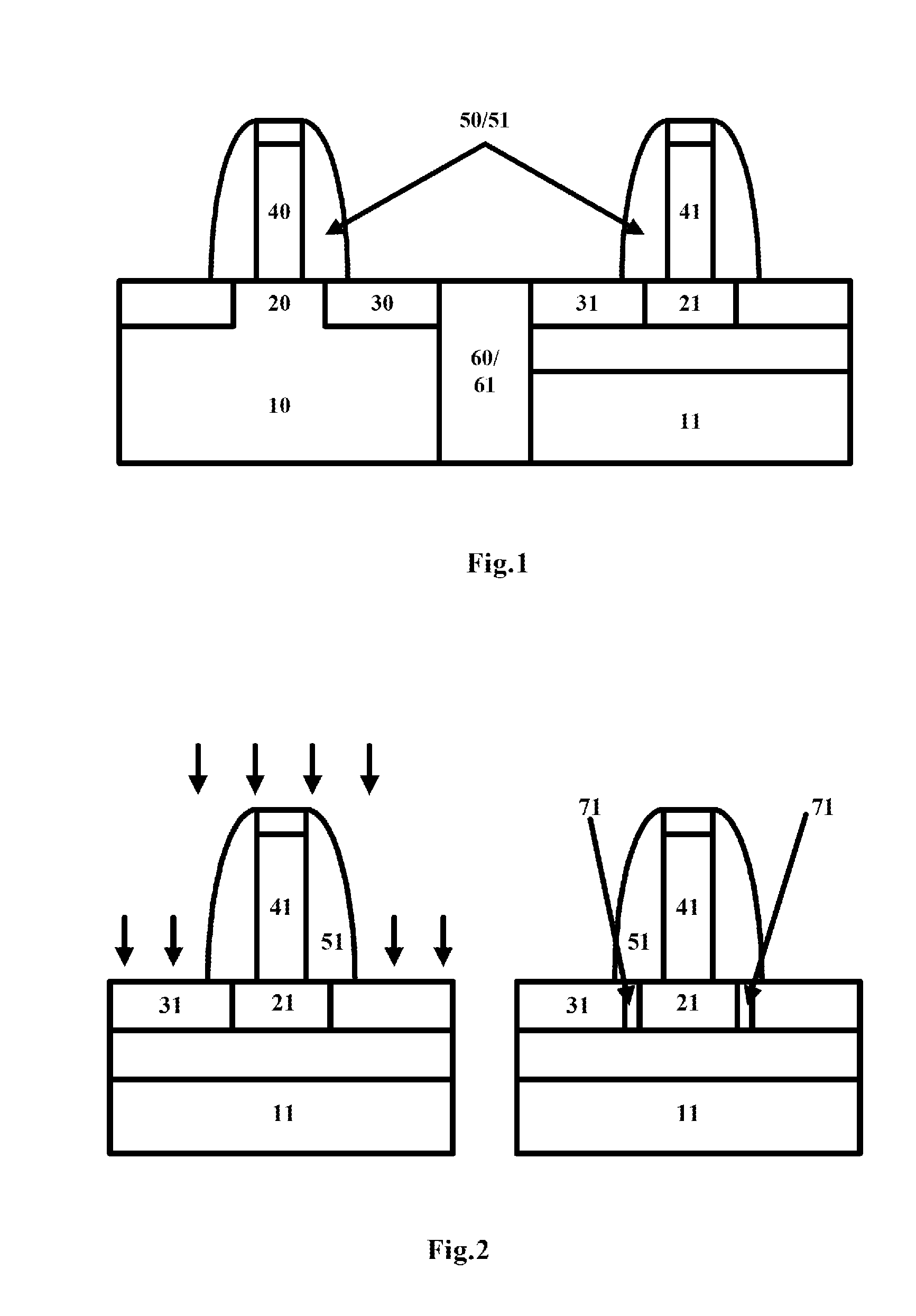
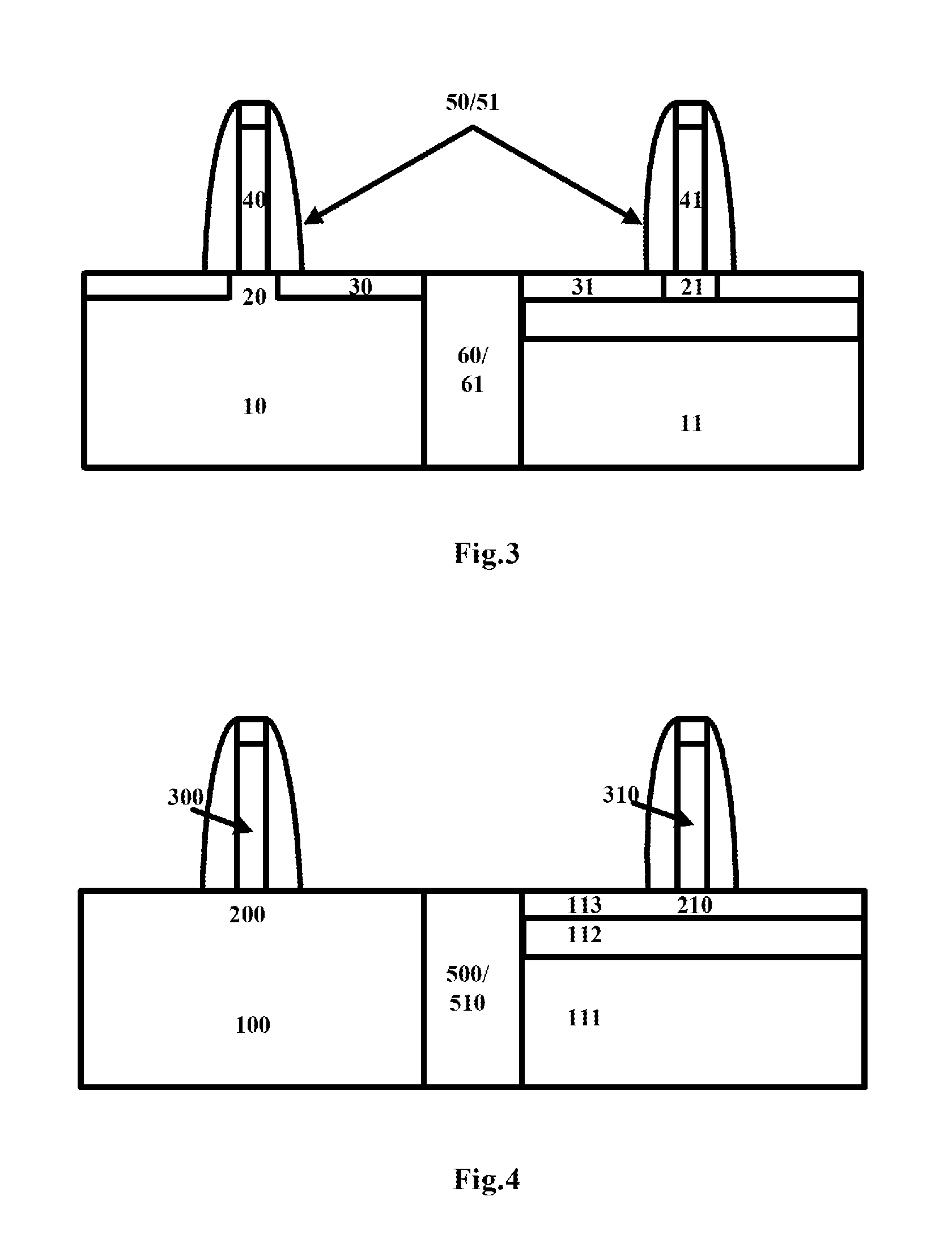
[0034]FIGS. 4-8 sequentially show cross-sectional views of device structures corresponding to the steps of a method for manufacturing a MOSFET with epitaxially grown ultrathin metal silicide source / drain in sequence. In these figures, the STIs are shown to be di...


PUM


Abstract

Disclosed is a semiconductor device, comprising a substrate, a channel region in the substrate, source / drain regions on both sides of the channel region, a gate structure on the channel region, and gate sidewall spacers formed on the sidewalls of the gate structure, characterized in that each of the source / drain regions comprises an epitaxially grown metal silicide region, and dopant segregation regions are formed at the interfaces between the epitaxially grown metal silicide source / drain regions and the channel region. By employing the semiconductor device and the method for manufacturing the same according to embodiments of the present invention, the Schottkey Barrier Height of the MOSFETs with epitaxially grown ultrathin metal silicide source / drain may be lowered, thereby improving the driving capability.

Description

TECHNICAL FIELD[0001]The present application relates to a semiconductor device, and more specifically, relates to a MOSFET structure that has epitaxially grown ultra-thin metal silicide source / drain and a method for manufacturing the same.BACKGROUND OF THE INVENTION[0002]In the current IT application field, with the increasing demand on the IC integration level and continuous proportional scaling of the traditional MOSFET, some parameters that are controllable through processing, such as channel length, gate oxide layer thickness, substrate doping concentration, etc., may be scaled proportionally. Although scaling the device size results in a greater process fluctuation, many physical parameters, such as the silicon forbidden band, the Fermi potential, interface states, oxide layer charges, thermoelectric potentials, and p-n junction built-in potentials, cannot be scaled proportionally. These will greatly deteriorate the performance of proportionally scaled device.[0003]One problem ...

Claims


Application Information

Patent Timeline
Patent Type & Authority Applications(United States)
IPC IPC(8): H01L29/78H01L21/336
CPCH01L29/47H01L29/7839H01L29/66772H01L29/66643
Inventor LUO, JUNZHAO, CHAO
Owner INST OF MICROELECTRONICS CHINESE ACAD OF SCI
Why Eureka
Try Eureka