Substrate for electronic device and electronic device

a technology for electronic devices and substrates, applied in the field of substrates for electronic devices and electronic devices, can solve the problems of increasing signal delay, increasing mounting area, and reducing production efficiency of electroplating, and achieve excellent heat dissipation characteristics

Active Publication Date: 2012-07-05
NAPRA
View PDF9 Cites 86 Cited by
  • Summary
  • Abstract
  • Description
  • Claims
  • Application Information

AI Technical Summary

Benefits of technology

[0014]It is an object of the present invention to provide a substrate for an electronic device with a heat transfer pathway having excellent heat dissipation characteristics and an electronic device using the same.

Problems solved by technology

However, this method not only requires the process of wire bonding but also increases the mounting area with the number of elements, so that the signal delay increases because of an increase in wiring length.
However, the electroplating decreases the production efficiency because of its inevitable long processing time.
Moreover, since the via typically has an aspect ratio of 5 or more and usually has a rugged inner wall surface, it is difficult to uniformly form a plating primary film over the inner wall surface of the via.
This produces a void or gap between the inner wall surface of the via and a plating film to be used as the through electrode, thereby causing an increase in electrical resistance, decreased reliability and so on.
Furthermore, there is also such a limit that the electrical resistance cannot be set lower than the inherent electrical resistance of Cu.
Still furthermore, the progress in improving the packaging density, the performance and the processing speed and reducing the size, the thickness and the weight of the electronic device because of the use of the TSV technology not only increases heat that will be generated by the operation but also makes it difficult to prepare a heat dissipation structure for it, so that the question of how to dissipate heat becomes a major issue.
If the heat dissipation is insufficient, accumulation of the generated heat leads to abnormal heat generation, impairing bonding strength of the electronic component and damaging reliability of the electrical connection or changing electrical characteristics of the electronic component and at worst, causing thermal runaway, thermal breakdown or the like.
However, any related art has a problem to be solved, such as improvement in heat dissipation characteristics, manufacturing cost reduction or the like.

Method used


Image

  • Substrate for electronic device and electronic device
  • Substrate for electronic device and electronic device
  • Substrate for electronic device and electronic device

Examples


embodiment 1

Light-Emitting Diode and Light-Emitting Device

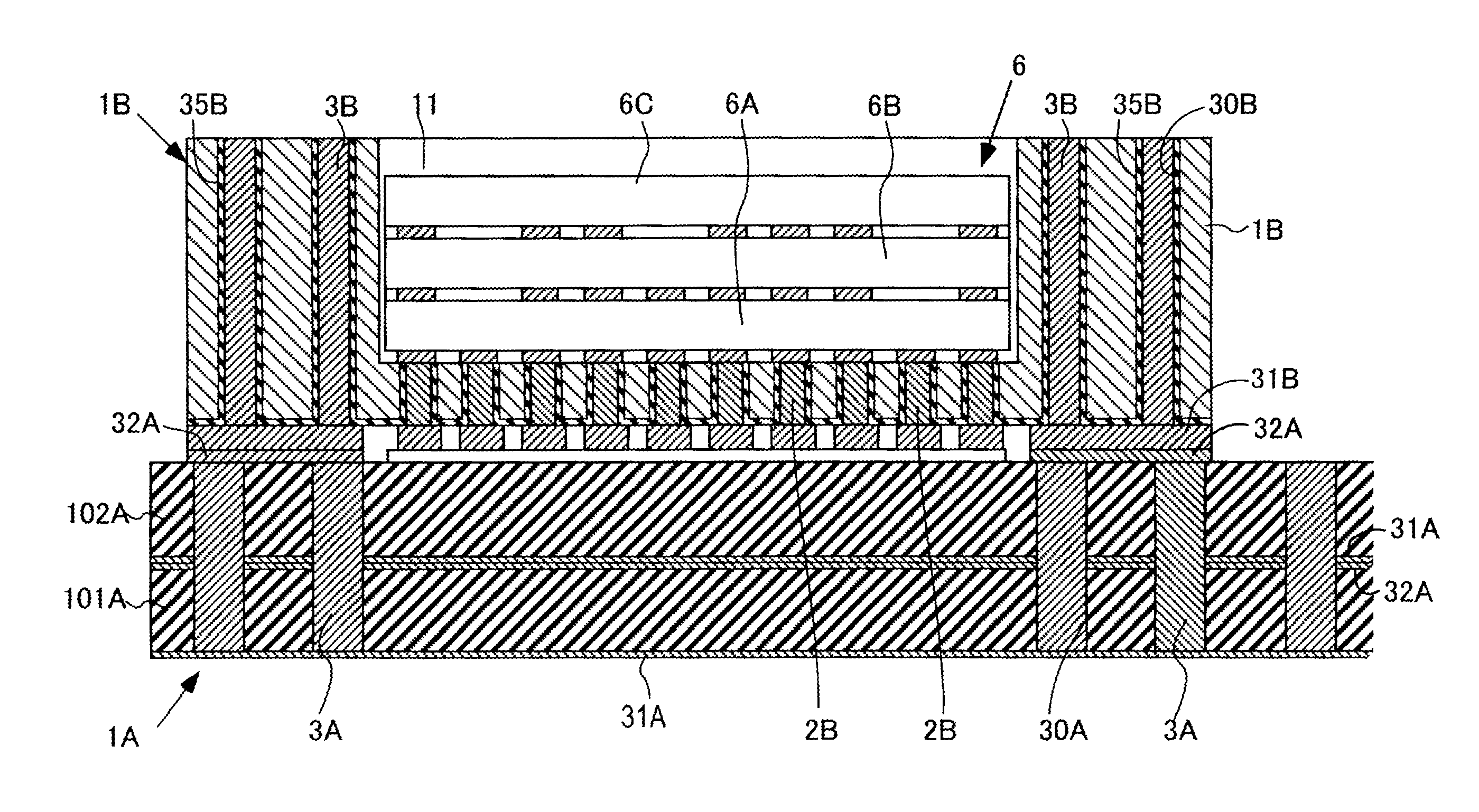
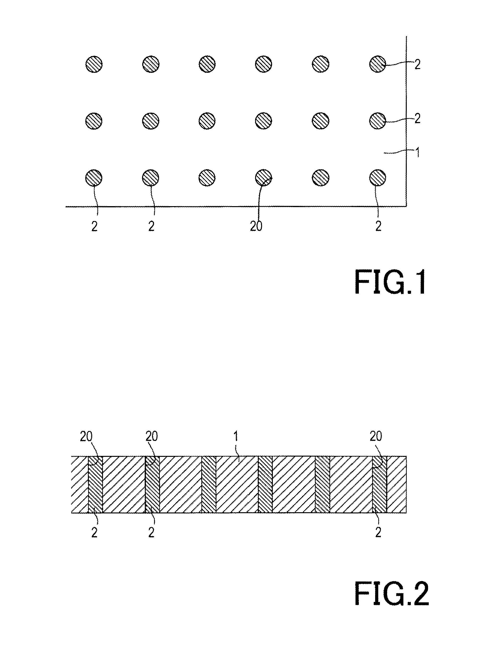
[0125]A light-emitting device shown in FIGS. 10 to 12 comprises a substrate 1 and a light-emitting element 6. The light-emitting element 6 is covered with a fluorescent layer 7. The substrate 1 serves as a so-called package, includes two through electrodes 2, 2 and a number of columnar heat sinks 3 and has a cavity 11 at one side thereof. Preferably, the substrate 1 includes Si as a main component. Alternatively, the substrate 1 may be an insulating resin substrate or an insulating ceramic substrate. In the figures, the substrate 1 has a rectangular outline but its shape is arbitrary. The cavity 11 of the substrate 1 is formed to surround the through electrodes 2, 2 at a distance, wherein a reflection film 8 such as an Al film, an Ag film or a Cr film is formed almost all along its inner side face by sputtering or the like. It is also possible to form an insulating film such as an oxide film beneath the reflection film 8.

[0126]The throug...

embodiment 2

Electronic Device or Electronic Equipment

[0189]The electronic element is not limited to the foregoing light-emitting element 6 but may be an active element, a passive component or a composite element thereof. It may also be one having the above-described various types of elements arranged into a three-dimensional multilayer structure based on the TSV technology or one having an interposer and the various types of elements combined into a three-dimensional multilayer structure.

[0190]Referring to FIG. 27, there is illustrated a circuit substrate suitable for mounting such an electronic element. In this figure, the components identical or similar to those illustrated in the foregoing figures are denoted by the same reference symbols. In FIG. 27, the number of through electrodes 2 is increased in accordance with the number of terminal electrodes of an electronic element to be mounted within the cavity 11. In addition, the cavity 11 has an inner side face extending substantially vertical...

embodiment 3

Other Devices

[0219]Referring to FIG. 33, there is illustrated a substrate having a number of columnar heat sinks 3. In this substrate 1, the tip of the columnar heat sink 3 is kept within a heat-resistant insulating organic or inorganic substrate 1, thereby leaving an insulating layer having a thickness of ΔH1 above it. That is, the columnar heat sink 3 is not required to pass through it. The thickness of ΔH1 can be determined arbitrarily.

[0220]Referring next to FIG. 34, there is illustrated a substrate 1 comprising an organic insulating substrate. The organic substrate 1 preferably comprises a heat-resistant material. Particularly preferred is one having a heat resistance of 300° C. or more. The organic substrate 1 has, on at least one side thereof, a metal layer 31, 32 such as of a Cu foil. The illustrated organic substrate 1 is a double-sided copper-clad substrate having the metal layers 31, 32 of a Cu foil on both sides thereof. Various types of such a double-sided copper-clad s...


PUM

PropertyMeasurementUnit
aspect ratioaaaaaaaaaa
lengthaaaaaaaaaa
lengthaaaaaaaaaa

Abstract

A substrate includes a plurality of through electrodes. The through electrode has a nanocomposite structure including a nm-sized carbon nanotube and is a casting formed by using a via formed in the substrate as a mold.

Description

BACKGROUND OF THE INVENTION[0001]1. Field of the Invention[0002]The present invention relates to a substrate for an electronic device and an electronic device.[0003]2. Description of the Related Art[0004]In electronic devices such as various scales of integrated circuits, various types of semiconductor elements and chips thereof, for example, there has been employed a method of disposing an element on a substrate and connecting them by means of wire bonding or the like. However, this method not only requires the process of wire bonding but also increases the mounting area with the number of elements, so that the signal delay increases because of an increase in wiring length.[0005]Therefore, there has been proposed a TSV (through-silicon-via) technology of providing a substrate with through-electrodes and replacing the conventional wire bonding with the through-electrodes. Japanese Unexamined Patent Application Publication Nos. 11-298138, 2000-228410, 2002-158191 and 2003-257891 disc...

Claims


Application Information

Patent Timeline
Patent Type & Authority Applications(United States)
IPC IPC(8): H05K7/20H05K1/16H05K1/11H05K1/03B82Y99/00
CPCH01L21/486H01L23/3677H01L23/49827H01L33/486H01L33/642H01L2924/09701H01L2224/16225H01L2933/0066H01L2224/48472H01L2924/01327H01L2924/12044H01L2924/00H01L23/49877H01L2924/181H01L2924/00012H05K1/02H05K3/40H05K3/46
Inventor SEKINE, SHIGENOBUSEKINE, YURINA
Owner NAPRA
Why Eureka
Try Eureka