

Electroluminescent device using azomethine-lithium-complex as electron injection layer
a technology of azomethinelithium and electron injection layer, which is applied in the field of compounds, can solve the problems that the use of metal schiff base complexes as electron injection materials for oleds is neither disclosed nor suggested, and achieves the effects of high deposition rate, improved performance and comparable performan
Active Publication Date: 2012-08-16
MERCK PATENT GMBH
View PDF8 Cites 2 Cited by
- Summary
- Abstract
- Description
- Claims
- Application Information
AI Technical Summary
Benefits of technology
[0014]The compounds of the above formula have the advantage that they give comparable performance to LiF when used as an electron injection layer, or in some embodiments better performance, but do not require the severe deposition conditions associated with LiF. Embodiments of the compounds can be handled in air and can be deposited by vacuum sublimation at temperatures significantly below that required for LiF (FIG. 13) e.g. below about 250° C. In addition to vacuum sublimation, embodiments of the compounds can be deposited by the organic vapour phase deposition (OVPD) process described inter alia by Universal Display Corporation in which organic films are deposited using an inert carrier gas to transfer films of organic material onto a cooled substrate in a hot-walled, low-pressure (typically 0.1-1 Torr) chamber. The process is stated to achieve relatively high deposition rates compared to vacuum sublimation, to permit better shadow mask patterning for forming arrays of pixels and to be useful for substrates of relatively large size. They can also be deposited by organo vapour jet printing (OVJP) which produces a collimated vapour jet of organic material and carrier gas and impinges the jet onto a cooled substrate to form a well defined deposit e.g. of individual pixels, see Shtein et al., Direct Mask-Free Patterning Of Molecular Organic Semiconductors Using Organic Vapor Jet Printing, J. Appl. Phys., 2004, 96(8), 4500 and WO 2005 / 043641 (Shtein et al.). Embodiments of the above compounds can be dissolved in organic solvents and deposited e.g. to form layers or pixels by solution coating e.g. spin coating or by ink jet printing (see WO 03 / 067679 and Bharathan et al., Polymer electroluminescent devices processed by inkjet printing, Alppl Phys. Lett., (1998) 72(21), 2660) the contents of which are incorporated herein by reference) the good solution processing properties being a significant advantage e.g. in the manufacture of polymer OLEDs, devices based on conductive polymers e.g. PEDOT. Ink jet printing has been reported using simple organic solvents e.g. an alcohol or chloroform. Preferred ink jet printing is using the piezo variant, and suitable solvents are dichloroethylene, thrichloroethylene, xylenes, N-methyl pyrrolidones, dioxane and other high boiling ethers, dichlorobnzene and polyhydroxy compounds. Similar solvents can be used in spin coating. In some embodiments, the compounds described above may when used as electron injection layers give rise to reduced voltage drift compared to the use of inorganic electron injectors such as LiF and increased device lifetime.
Problems solved by technology
However, the use of metal Schiff base complexes as electron injection materials for OLEDs is neither disclosed nor suggested by Herron et al.
Method used
View moreImage
Smart ImageViewing Examples

Examples
example 2
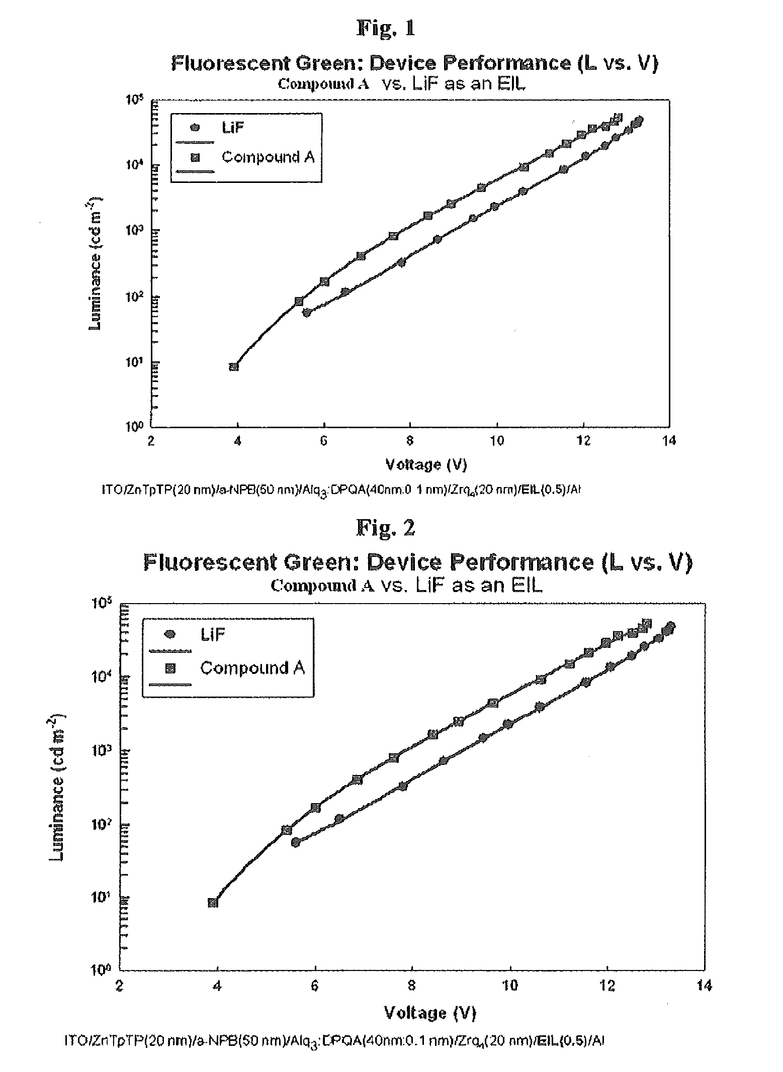
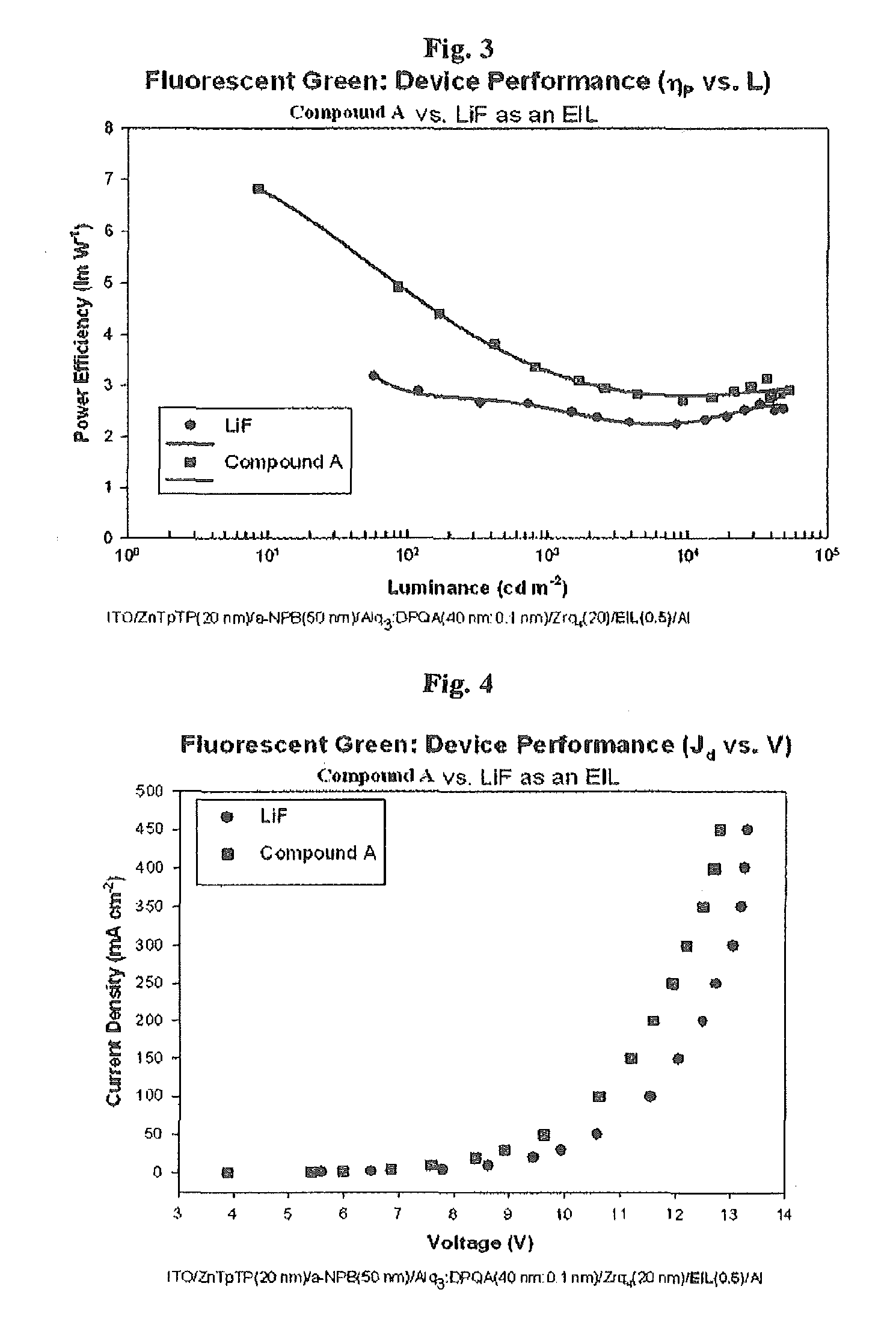
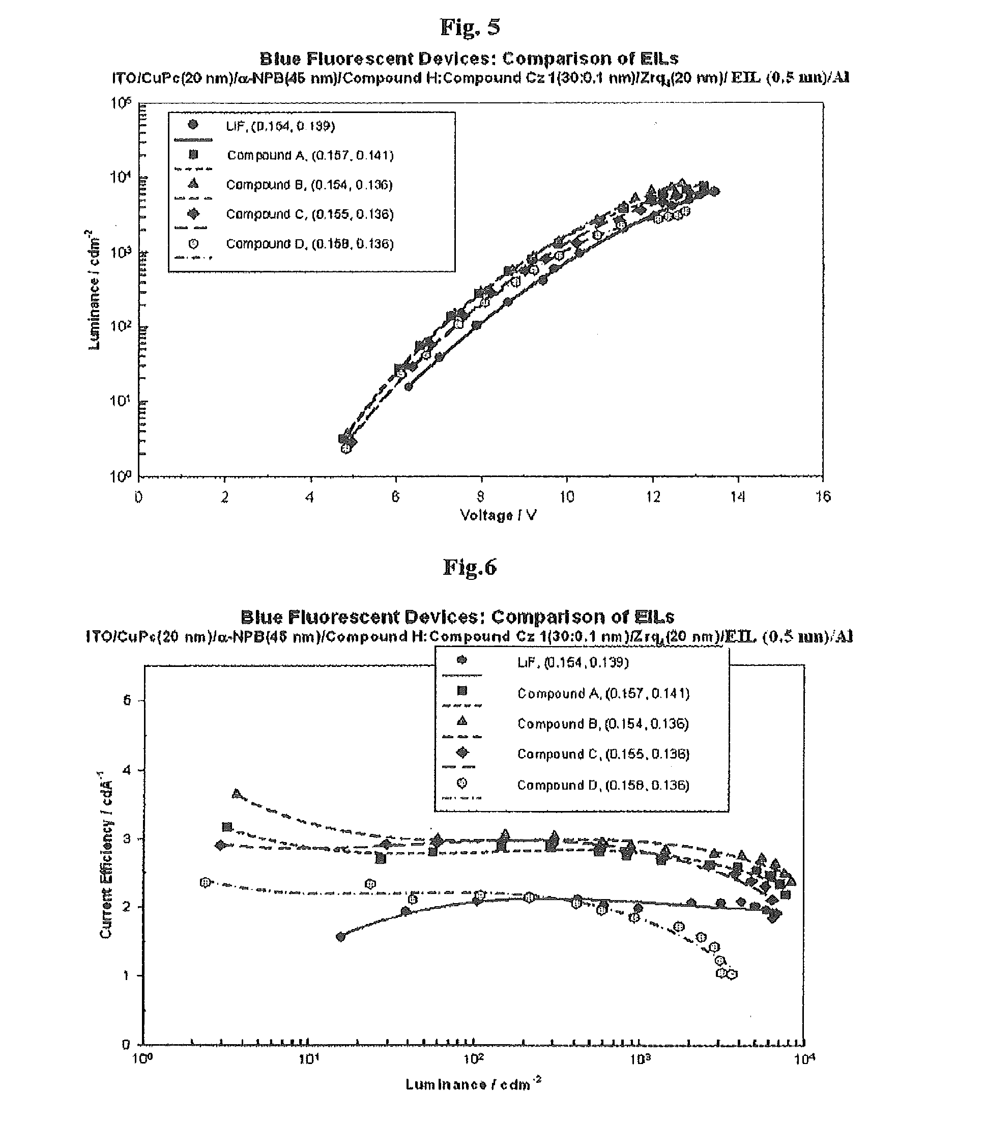
[0151]Further devices in which the electron injection layer was a compound made as described above were manufactured and evaluated in relation to similar devices made using Lif as the injection layer. Performance results are shown in FIGS. 5-12. Compounds H and Cz1 used in the electroluminescent layer in some tests are shown below:
Login to View More PUM
| Property | Measurement | Unit |
|---|---|---|
| pressure | aaaaa | aaaaa |
| temperatures | aaaaa | aaaaa |
| temperatures | aaaaa | aaaaa |
Abstract
In OLEDs, improved efficiency is obtained by compounds which can form inter alia electron injection layers of the formula (I)whereinR1 is a 1-5 ring aryl (including polycyclic), aralkyl or heteroaryl group which is optionally substituted with one or more C1-C4 alkyl, alkoxy or cyano;R2 and R3 together form a 1-5 ring aryl (including polycyclic), aralkyl or heteroaryl group which is optionally substituted with C1-C4 alkyl, alkoxy or cyano;R4 is hydrogen, C1-C4 alkyl or aryl; andAr is monocyclic, bicyclic or tricyclic aryl or heteroaryl which is optionally substituted with one or more C1-C4-alkyl or alkoxy groups, or an oligomer thereof.
Description
FIELD OF THE INVENTION[0001]This invention relates to novel compounds, comprising said compounds and one or more dopants, and to their use in electro-optical or opto-electronic devices, inter alia optical light emitting devices, for example in an electron injection layer.BACKGROUND TO THE INVENTION[0002]Hung et al., “Recent progress of molecular organic electroluminescent materials and devices”, Materials Science and Engineering, R 39 (2002), 143 -222 disclose that bilayer cathodes for OLEDs based e.g. on a thin (0.1-1.0 nm) LiF layer between an aluminium cathode and an aluminium quinolate electron transport layer exhibit significantly improved I-V characteristics and EL efficiencies. They explain that in OLEDs, the majority carriers are holes owing to their higher mobility and smaller injection barrier. Therefore, lowering the barrier height to electron injection is especially important as it leads to a better balance of electron and hole currents and results in a dramatic increase...
Claims
Login to View More Application Information
Patent Timeline
 Patent Type & AuthorityApplications(United States)
IPC IPC(8): H01L51/54H01B1/12C07F1/02H10K99/00
CPCC07C251/24Y10S428/917C09K11/06C09K2211/1007C09K2211/1011C09K2211/1014C09K2211/1029C09K2211/1037C09K2211/1044C09K2211/1059C09K2211/1088C09K2211/1092C09K2211/181C09K2211/185H01L51/005H01L51/0072H01L51/0077H01L51/5092H05B33/14C07C255/61H10K85/60H10K85/30H10K85/6572H10K50/171C07F1/02H10K50/12
InventorKATHIRGAMANATHAN, POOPATHYCHAN, YUN FU
OwnerMERCK PATENT GMBH