Method for forming oxide semiconductor film and method for manufacturing semiconductor device

a semiconductor film and oxide technology, applied in the direction of semiconductor devices, basic electric elements, electrical appliances, etc., can solve the problems of the semiconductor film's semiconductor characteristics, and achieve the effects of reducing the amount of hydrogen contained, favorable semiconductor characteristics, and favorable electric characteristics

Active Publication Date: 2012-09-27
SEMICON ENERGY LAB CO LTD
View PDF12 Cites 26 Cited by
  • Summary
  • Abstract
  • Description
  • Claims
  • Application Information

AI Technical Summary

Benefits of technology

[0023]Further, by applying the method for forming the oxide semiconductor film from which hydrogen is released, a semiconductor device can be manufactured.
[0024]According to one embodiment of the present invention, a method for forming an oxide semiconductor film in which t...

Problems solved by technology

As described above, when hydrogen enter the oxide semiconductor film and conductivity is...

Method used


Image

  • Method for forming oxide semiconductor film and method for manufacturing semiconductor device
  • Method for forming oxide semiconductor film and method for manufacturing semiconductor device
  • Method for forming oxide semiconductor film and method for manufacturing semiconductor device

Examples


embodiment 1

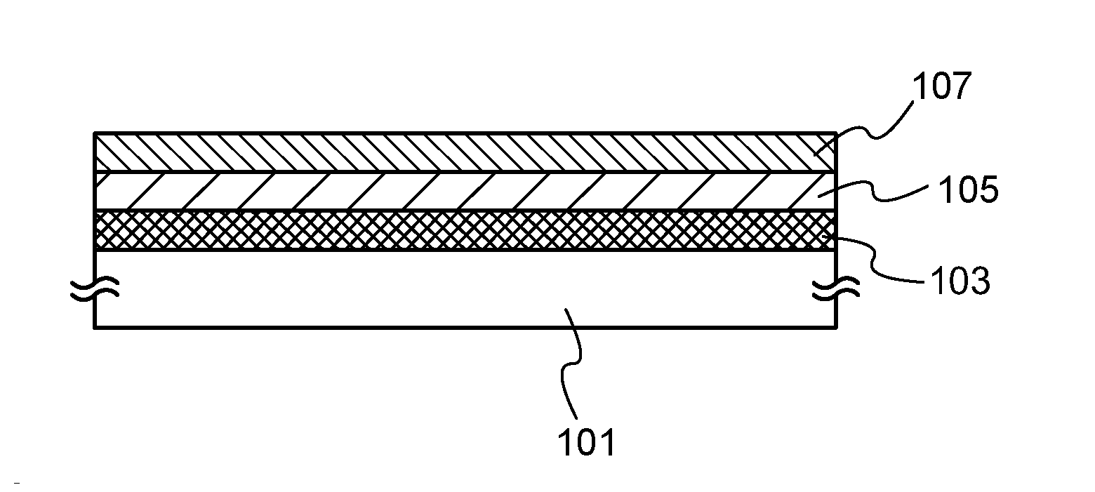
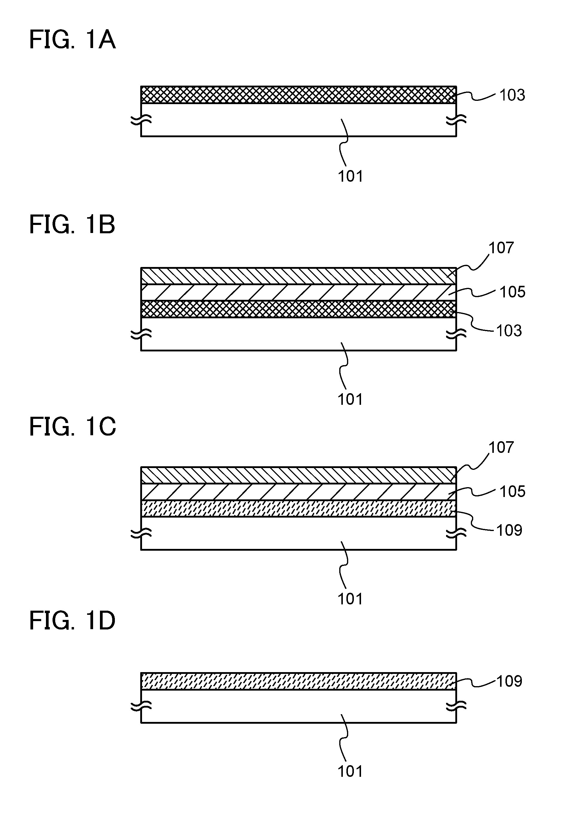
[0040]In this embodiment, a method for forming an oxide semiconductor film of one embodiment of the present invention will be described. Specifically, a method for forming an oxide semiconductor film from which hydrogen is released will be described with reference to FIGS. 1A to 1D.

[0041]There is no particular limitation on a material and the like of a substrate 101 as long as the material has heat resistance high enough to withstand at least heat treatment performed later. For example, a glass substrate, a ceramic substrate, a quartz substrate, a sapphire substrate, or the like can be used as the substrate 101. Further alternatively, a single crystal semiconductor substrate or a polycrystalline semiconductor substrate made of silicon, silicon carbide, or the like, a compound semiconductor substrate made of silicon germanium or the like, an SOI substrate, or the like may be used as the substrate 101. Furthermore, any of these substrates provided with a semiconductor element may be u...

embodiment 2

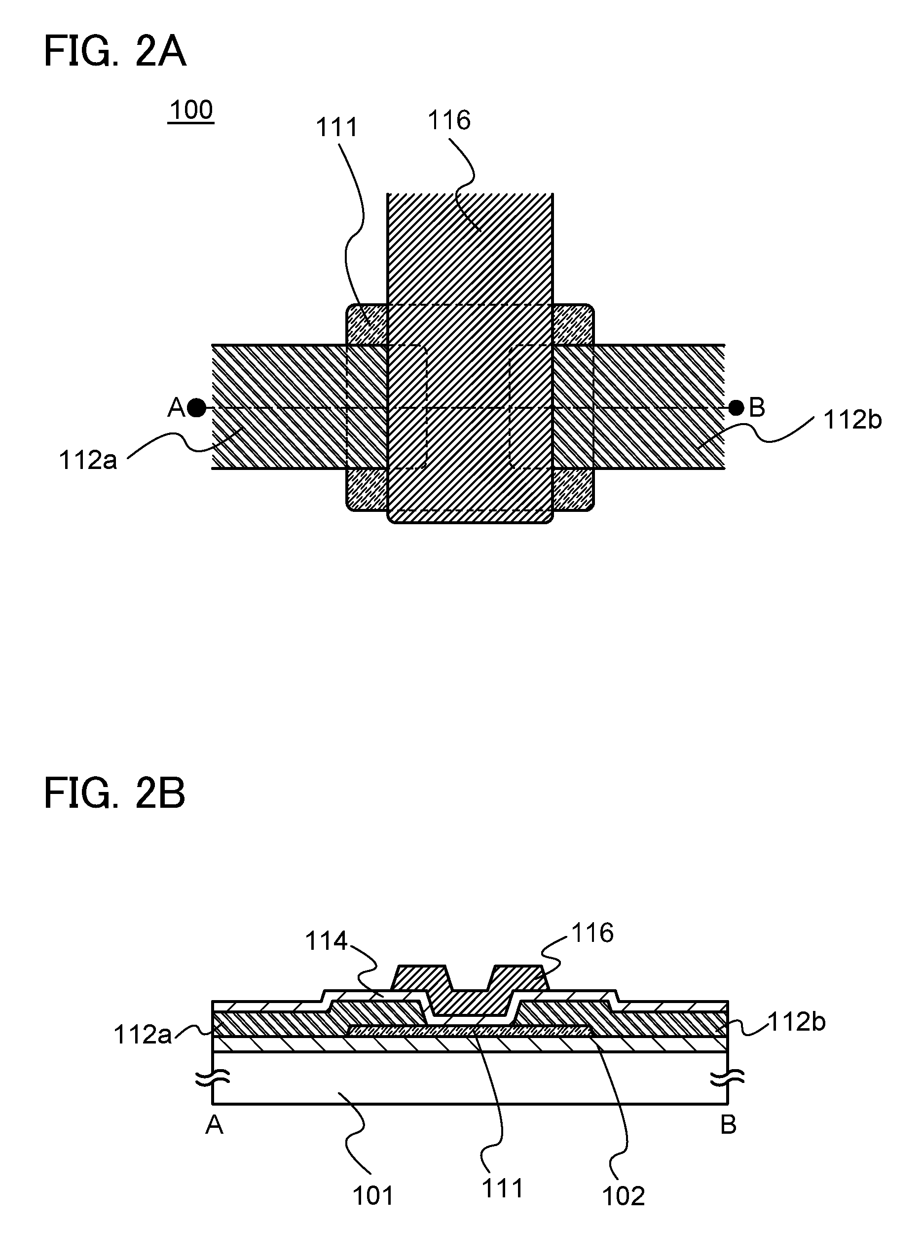
[0090]In this embodiment, a method for manufacturing a semiconductor device, to which the method for forming an oxide semiconductor film described in Embodiment 1 is applied, will be described. Here, a method for manufacturing a transistor is described as an example.

[0091]There is no particular limitation on a structure of a transistor to which the method for forming an oxide semiconductor film described in Embodiment 1 is applied. Any of a top gate structure, a bottom gate structure or a dual gate structure can be employed. Specifically, any of a top-gate top-contact structure, a top-gate bottom-contact structure, a bottom-gate top-contact structure, or a bottom-gate bottom-contact structure can be employed.

[0092]In this embodiment, as an example, the case where the method for forming an oxide semiconductor film described in Embodiment 1 is applied to a top-gate top-contact transistor is described. Note that the transistor is referred to as a transistor 100, and a structure and a m...

embodiment 3

[0136]In this embodiment, a liquid crystal display device manufactured using the transistor described in Embodiment 2 will be described. Note that an example in which one embodiment of the present invention is applied to a liquid crystal display device will be described in this embodiment; however, the present invention is not limited to this embodiment. For example, application of one embodiment of the present invention to an electroluminescence (EL) display device which is one of light-emitting devices is readily conceived by those skilled in the art.

[0137]FIG. 4 is a circuit diagram of an active matrix liquid crystal display device. The liquid crystal display device includes source lines SL_1 to SL_a, gate lines GL_1 to GL_b, and a plurality of pixels 2200. Each pixel 2200 includes a transistor 2230, a capacitor 2220, and a liquid crystal element 2210. The plurality of pixels 2200 with such a structure forms a pixel portion of the liquid crystal display device. In the case where ...


PUM


Abstract

A method for forming an oxide semiconductor film having favorable semiconductor characteristics is provided. In addition, a method for manufacturing a semiconductor device having favorable electric characteristics, with use of the oxide semiconductor film is provided. A method for forming an oxide semiconductor film including the steps of forming an oxide semiconductor film, forming a hydrogen permeable film over and in contact with the oxide semiconductor film, forming a hydrogen capture film over and in contact with the hydrogen permeable film, and releasing hydrogen from the oxide semiconductor film by performing heat treatment. Further, in a method for manufacturing a semiconductor device, the method for forming an oxide semiconductor film is used.

Description

BACKGROUND OF THE INVENTION[0001]1. Field of the Invention[0002]The present invention relates to a method for forming an oxide semiconductor film and a method for manufacturing a semiconductor device with use of the method for forming an oxide semiconductor film.[0003]In this specification, a semiconductor device generally refers to a device which can function by utilizing semiconductor characteristics; an electro-optical device, a semiconductor circuit, and an electronic device are all included in the category of the semiconductor device.[0004]2. Description of the Related Art[0005]In recent years, transistors which are used for many liquid crystal display devices and light-emitting display devices typified by flat panel displays have been formed over glass substrates and using a silicon semiconductor such as amorphous silicon or polycrystalline silicon.[0006]Instead of the silicon semiconductor, a technique in which an oxide semiconductor that is a metal oxide having semiconductor...

Claims


Application Information

Patent Timeline
IPC IPC(8): H01L21/42
CPCH01L29/66969H01L29/7869
Inventor IMOTO, YUKIMARUYAMA, TETSUNORITAKAYAMA, TORU
Owner SEMICON ENERGY LAB CO LTD
Why Eureka
Try Eureka