Post deposition treatments for CVD cobalt films

a cobalt film and post-deposition treatment technology, applied in the direction of semiconductor devices, semiconductor/solid-state device details, electrical apparatus, etc., can solve the problems of difficult deformation of feature geometry, difficult to fill these features without, and difficult to ensure the formation of interconnections

Inactive Publication Date: 2012-10-04
APPLIED MATERIALS INC
View PDF1 Cites 79 Cited by
  • Summary
  • Abstract
  • Description
  • Claims
  • Application Information

AI Technical Summary

Benefits of technology

[0014]In another embodiment, a conductive metallic layer may be deposited, plated, or otherwise formed on or over the cobalt oxide layer disposed over the crystalline cobalt film during another optional step of the process. The conductive metallic layer may contain a metal such as aluminum, copper, titanium, alloys thereof, or combinations thereof. Subsequently, the conductive metallic layer contained on the substrate may be heated to a predetermined temperature while metal from the conductive metallic layer diffuses into the cobalt oxide layer and the crystalline cobalt film during a thermal annealing process. The diffused metal from the conductive metallic layer reduces the resistivity of the cobalt oxide layer and the crystalline cobalt film. During the thermal annealing process, the conductive metallic layer may be heated to a temperature within a range from about 200° C. to about 600° C. The metal of the conductive metallic layer may reflow to form void-free gap fill during the thermal annealing process.

Problems solved by technology

Filling these features without creating voids or deforming the feature geometry is more difficult when the features have higher aspect ratios.
Reliable formation of interconnects is also more difficult as manufacturers strive to increase circuit density and quality.
Each processing method may increase the likelihood of problematic issues such as cobalt conductivity, cobalt crystalline structure deformation, and agglomeration.
Physical vapor deposition (PVD), chemical vapor deposition (CVD), atomic layer deposition (ALD), electrochemical plating (ECP), electroless deposition, and other deposition techniques have been utilized for depositing cobalt materials and layers, however, such cobalt layers generally suffer with the aforementioned issues.
Cobalt layers deposited by PVD are often non-conformal and have other irregularities that affect device performance and stability.
Also, high aspect ratio features usually develop voids during the deposition of cobalt materials by PVD or CVD.
Also, the cobalt layers deposited by ECP and electroless deposition processes may often have relative high resistivity and poor conformal films.

Method used


Image

  • Post deposition treatments for CVD cobalt films
  • Post deposition treatments for CVD cobalt films
  • Post deposition treatments for CVD cobalt films

Examples


Embodiment Construction

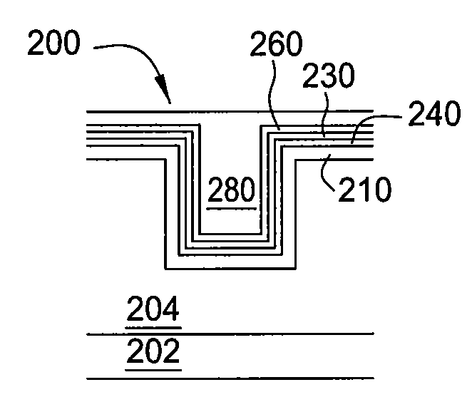
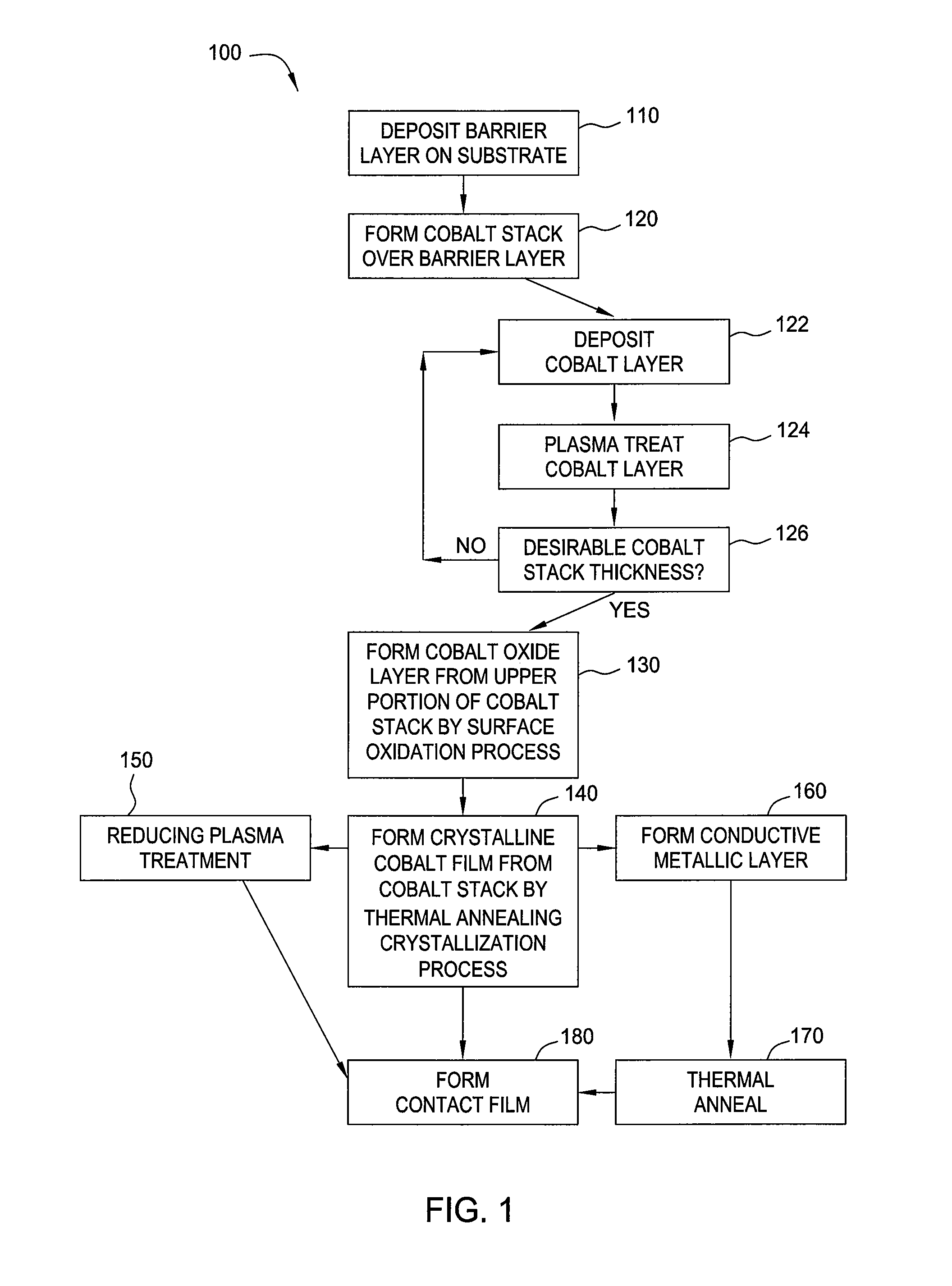
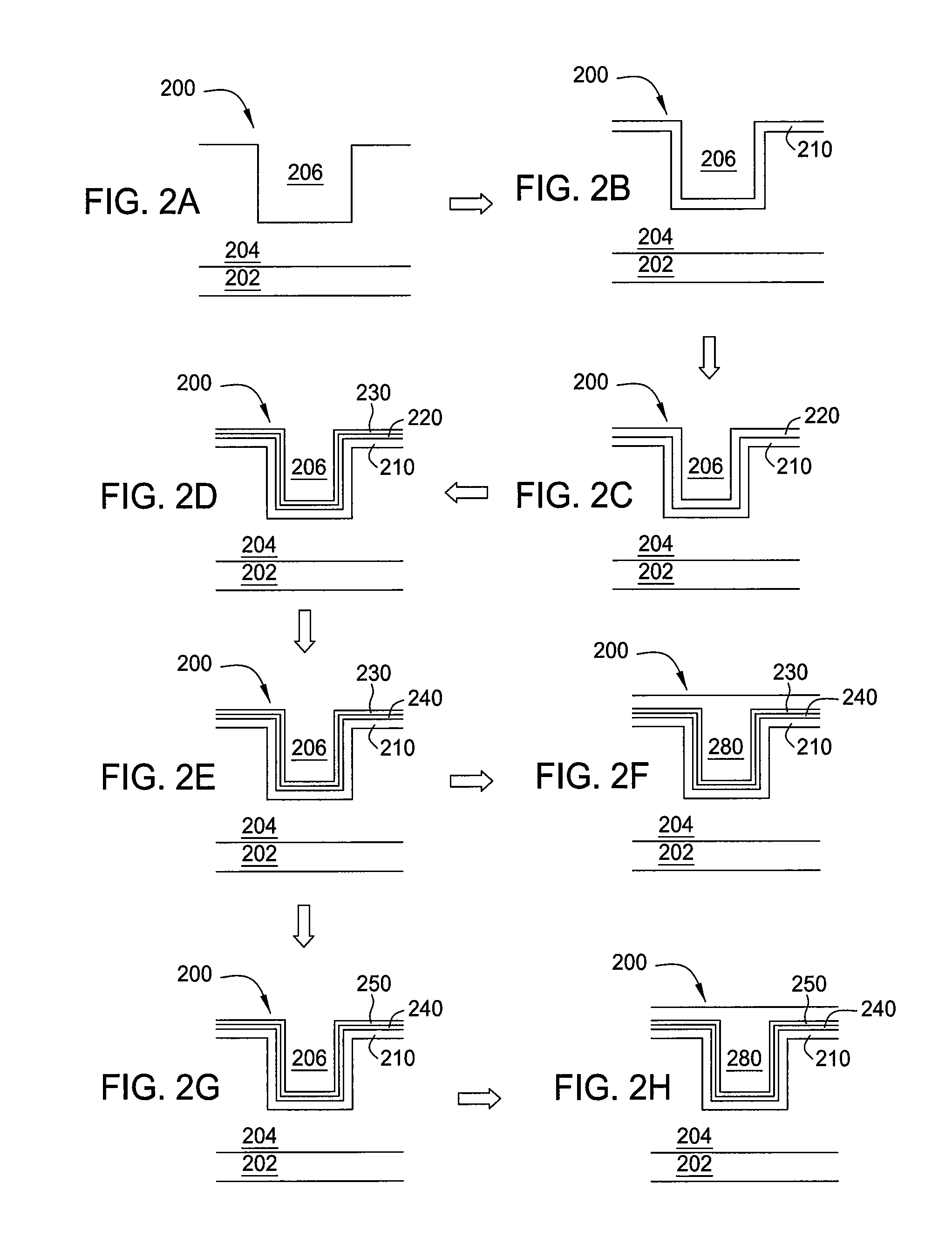
[0024]Embodiments of the invention provide methods for forming and treating materials on a substrate used for metal gate applications and other semiconductor, solar, or electronic device applications. In one embodiment, a method for depositing materials on a substrate surface is provided and includes forming a cobalt stack on or over a barrier layer disposed on a substrate by depositing a cobalt layer during a deposition process, exposing the cobalt layer to a plasma to form a plasma-treated cobalt layer during a plasma process, and repeating the cobalt deposition process and the plasma treatment process to form the cobalt stack. Generally, the cobalt stack contains a plurality of plasma-treated cobalt layers, but alternatively, the cobalt deposition process and the plasma treatment process may be performed once to form a single plasma-treated cobalt layer as the cobalt stack.

[0025]The method further includes exposing the cobalt stack to an oxygen source gas to form a cobalt oxide l...


PUM

PropertyMeasurementUnit
crystallization temperatureaaaaaaaaaa
temperatureaaaaaaaaaa

Abstract

Embodiments of the invention provide methods for forming materials on a substrate used for metal gate and other applications. In one embodiment, a method includes forming a cobalt stack over a barrier layer disposed on a substrate by depositing a cobalt layer during a deposition process, exposing the cobalt layer to a plasma to form a plasma-treated cobalt layer during a plasma process, and repeating the cobalt deposition process and the plasma process to form the cobalt stack containing a plurality of plasma-treated cobalt layers. The method further includes exposing the cobalt stack to an oxygen source gas to form a cobalt oxide layer from an upper portion of the cobalt stack during a surface oxidation process and heating the remaining portion of the cobalt stack to a temperature within a range from about 300° C. to about 500° C. to form a crystalline cobalt film during a thermal annealing crystallization process.

Description

BACKGROUND OF THE INVENTION[0001]1. Field of the Invention[0002]Embodiments of the invention generally relate to a metallization process for manufacturing electronic and semiconductor devices, more particularly, embodiments relate to methods for depositing and treating cobalt films on a substrate.[0003]2. Description of the Related Art[0004]Currently, cobalt is a metal of choice for use in multilevel metallization processes that are crucial to device manufacturing, especially for the PMOS work function layers of metal-oxide-semiconductor field-effect transistor (MOSFET) as well as wetting layer for direct metal gap fill. The multilevel interconnect features that drive the manufacturing processes have high aspect ratio apertures including contacts, vias, lines, gaps, and other features. Filling these features without creating voids or deforming the feature geometry is more difficult when the features have higher aspect ratios. Reliable formation of interconnects is also more difficul...

Claims


Application Information

Patent Timeline
Patent Type & Authority Applications(United States)
IPC IPC(8): H01L21/283B82Y40/00
CPCH01L21/76885H01L21/7681H01L21/76834H01L21/02697H01L21/76856H01L21/76873H01L21/7685B82Y40/00H01L21/28556H01L21/28562H01L23/53223H01L23/53238H01L23/53266H01L21/76846H01L21/76858H01L21/76862H01L21/76864H01L21/76877H01L2924/0002H01L2924/00
Inventor LEI, YUFU, XINYUSUBRAMANI, ANANTHAGANGULI, SESHADRIGANDIKOTA, SRINIVAS
Owner APPLIED MATERIALS INC
Why Eureka
Try Eureka