

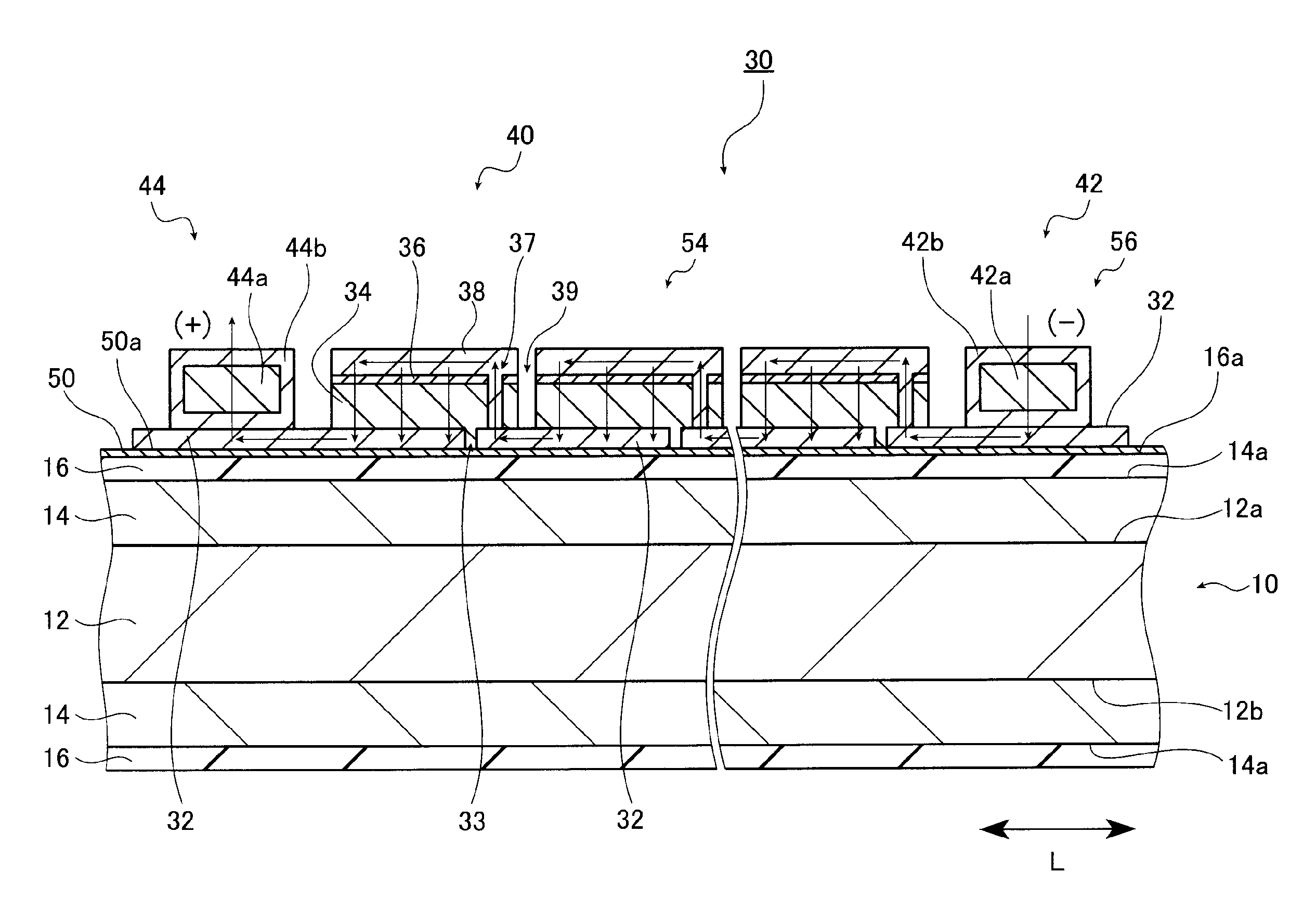
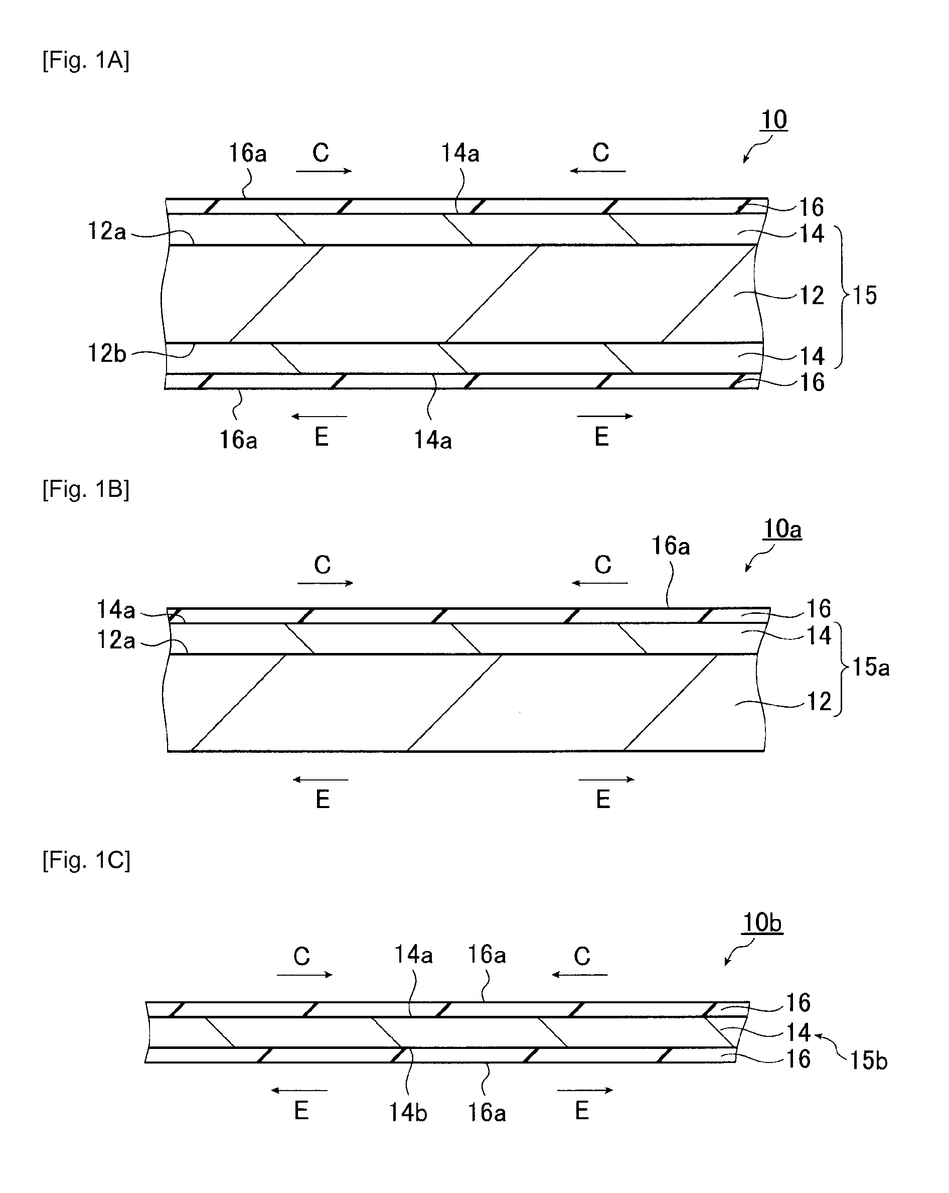
Metal substrate with insulation layer and manufacturing method thereof, semiconductor device and manufacturing method thereof, solar cell and manufacturing method thereof, electronic circuit and manufacturing method thereof, and light-emitting element and manufacturing method thereof
a technology of metal substrates and manufacturing methods, applied in the direction of surface reaction electrolytic coatings, porous dielectrics, light support devices, etc., can solve the problems of weak adhesion strength between aluminum and organic materials, low thermal conductivity of organic materials, and low improvement conductivity. , to achieve the effect of excellent cracking resistance, good insulation properties, and high reliability without cracking
- Summary
- Abstract
- Description
- Claims
- Application Information
AI Technical Summary
Benefits of technology
Problems solved by technology
Method used
Image

Examples
example 1
[0342]Example 1 of the metal substrate with an insulation layer of the present invention will be specifically described below.
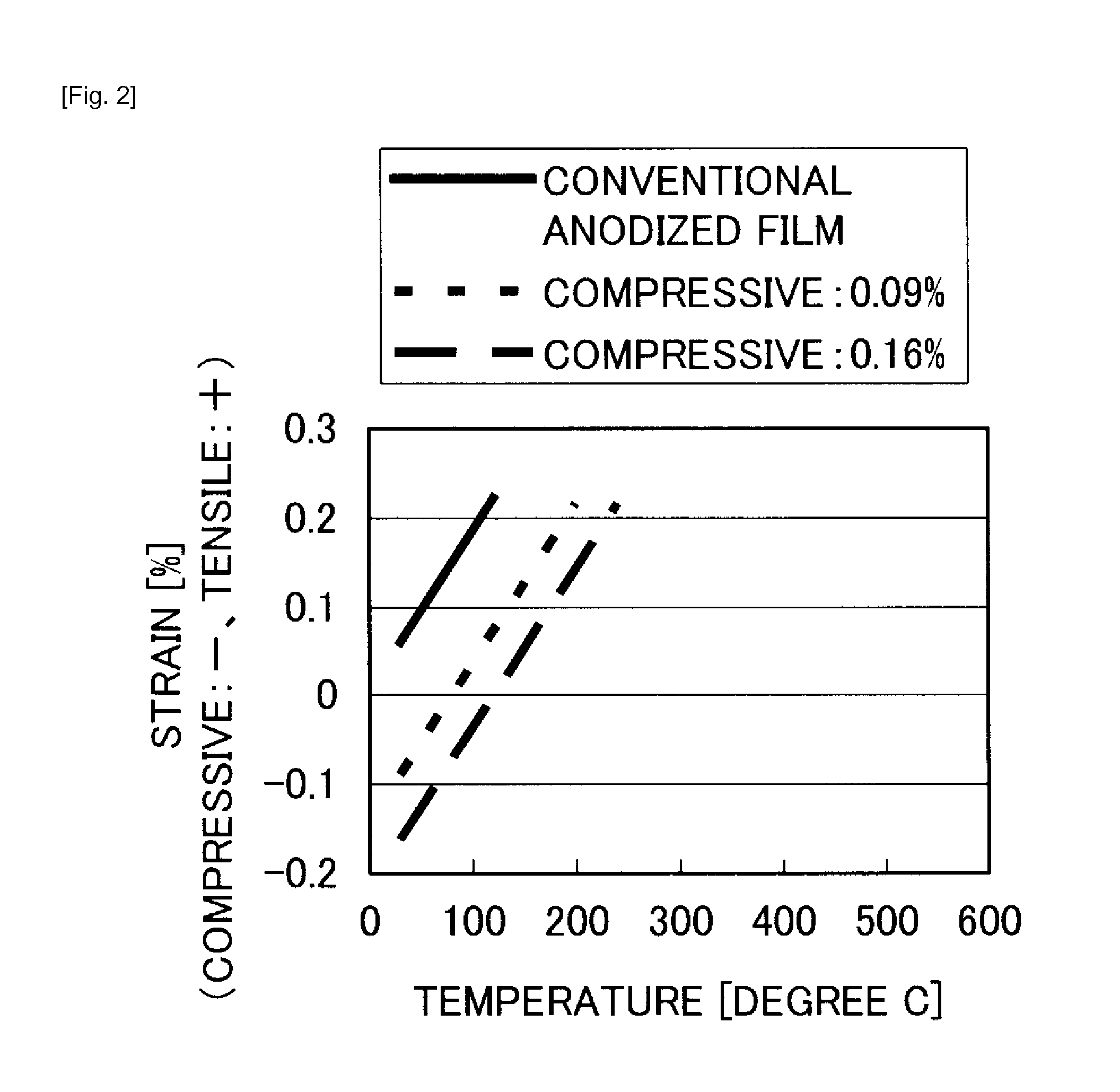
[0343]In this Example 1, working example numbers 1 through 68 and comparison example numbers 1 through 22 shown below were manufactured, and the magnitude of strain and Young's modulus of the anodized film which forms the insulation layer were measured for each, and internal stress was calculated. Further, a thermal strain test and an insulation breakdown test were performed, and thermal strain resistance and insulation breakdown voltage were assessed.
[0344]Note that in working example numbers 33 through 68, metal substrates with an insulation layer were each produced using a composite substrate of aluminum and another metal, and the anodized film that forms the insulation layer was assessed.
[0345]The results of thermal strain resistance and insulation breakdown voltage of working example numbers 1 through 68 and comparison example numbers 1 through 22 are sh...
example 2
[0364]Example 2, anodization treatment was performed on metal substrates under the conditions shown in Tables 7 and 8, forming anodized films to serve as insulation layers. After that, annealing treatment was performed under the annealing conditions shown in Tables 7 and 8. By annealing the anodized films in this way, metal substrates with an insulation layer of working example numbers 70 through 111 and comparison example numbers 30 through 32 shown in Tables 7 and 8 were manufactured. Then, for each of the metal substrates with an insulation layer of working example numbers 70 through 111 and comparison example numbers 30 through 32, the magnitude of strain and Young's modulus of the anodized film which forms the insulation layer were measured, and internal stress was calculated. Further, a thermal strain test and an insulation breakdown test were performed, and thermal strain resistance and insulation breakdown voltage were assessed.
[0365]Note that in working example numbers 82 t...
example 3
[0375]Example 3, the metal substrates with an insulation layer of working example numbers 120 through 125 and comparison example numbers 40 through 43 shown below were manufactured, and the magnitude of strain and Young's modulus of the anodized film were measured for each, and internal stress was calculated. The results are shown in Table 11.
[0376]Further, a bending strain test was performed for the substrates with an insulation layer of working example numbers 120 through 125 and comparison example numbers 40 through 43, and the reduction in bending strain resistance was assessed. The results are shown in Table 12.
[0377]In this example 3, anodization treatment was performed under the conditions shown in Table 11 on the metal substrates shown in Table 11, thereby forming an anodized film serving as an insulation layer, and the substrates with an insulation layer of working example numbers 120 through 125 and comparison example numbers 40 through 43 were thus obtained. In this examp...
PUM
| Property | Measurement | Unit |
|---|---|---|
| pKa | aaaaa | aaaaa |
| time | aaaaa | aaaaa |
| thickness | aaaaa | aaaaa |
Abstract
Description
Claims
Application Information