Method for fabricating surrounding-gate silicon nanowire transistor with air sidewalls

a silicon nanowire transistor and air sidewall technology, applied in the field of manufacturing technology of ultra-, can solve the problems of increasing the sub-threshold slope, unnegligible issue, fringing capacitance between the gate and the source/drain, etc., and achieves the effect of increasing the transient response characteristic of the device and reducing the parasitic capacitan

Active Publication Date: 2012-11-29
SEMICON MFG INT (SHANGHAI) CORP +1
View PDF5 Cites 14 Cited by
  • Summary
  • Abstract
  • Description
  • Claims
  • Application Information

AI Technical Summary

Benefits of technology

[0038]The beneficial effects of the invention lie in that, the method for fabricating the surrounding-gate silicon nanowire transistor with air sidewalls according to the invention is compatible with the CMOS

Problems solved by technology

As a device size has been reduced to a deep sub-micrometer, gate control capability of a conventional planar transistor is getting down, and a short channel effect is becoming more and more obvious, thus leading to a series of problems, such as drift of threshold voltage, increase of sub-threshold slope and leakage current in sub-threshold region, drain induced barrier low

Method used


Image

  • Method for fabricating surrounding-gate silicon nanowire transistor with air sidewalls
  • Method for fabricating surrounding-gate silicon nanowire transistor with air sidewalls
  • Method for fabricating surrounding-gate silicon nanowire transistor with air sidewalls

Examples


embodiment 1

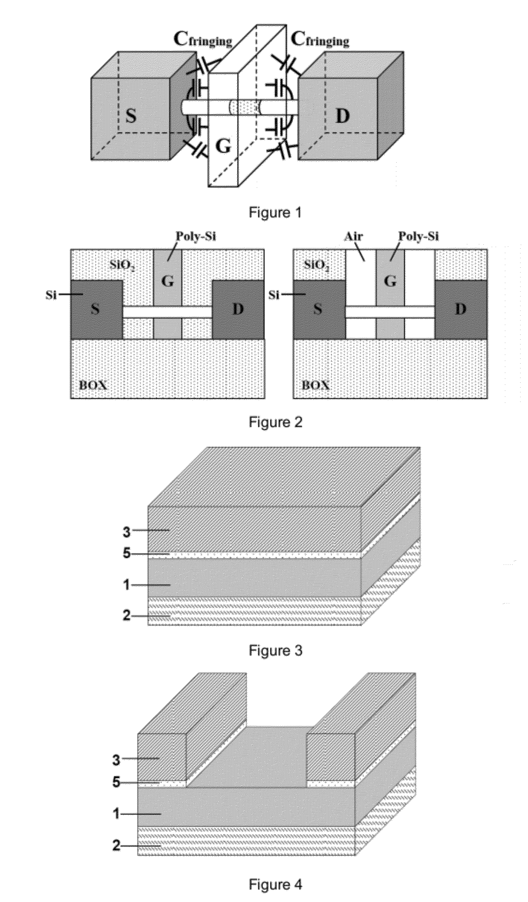
[0043]a process flow for fabricating a surrounding-gate silicon nanowire device with air sidewalls are as follows.

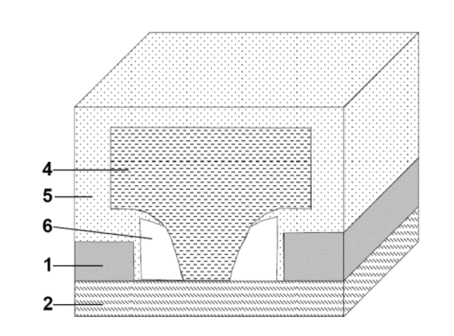
[0044]Starting from a SOI substrate (a thickness of a Si layer over a buried oxide layer is 2500 Å):

[0045]1. A silicon island isolation is performed.

[0046]2. A SiO2 layer is deposited with a thickness of 300 Å by using a low pressure chemical vapor deposition (LPCVD).

[0047]3. A SiN layer is deposited with a thickness of 1500 Å by using a low pressure chemical vapor deposition (LPCVD), as shown in FIG. 3.

[0048]4. A photolithography process is performed to define a channel region and a large source / drain region.

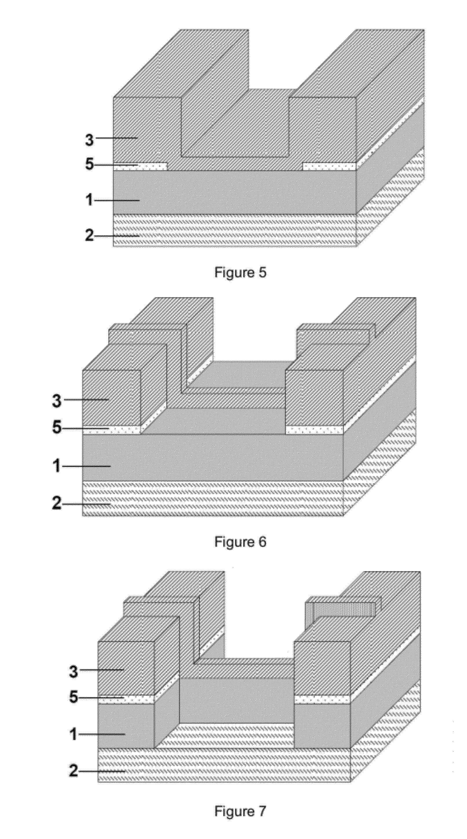
[0049]5. As shown in FIG. 4, the SiN layer is etched by 1500 Å and the SiO2 layer is etched by 300 Å by using a reactive ion etching (RIE) technology, so as to form a hard mask for the large source / drain region; and then the photoresist is removed.

[0050]6. A SiN layer is deposited with a thickness of 300 Å, as shown in FIG. 5.

[0051]7. A photolithography process is p...

embodiment 2

[0072]to the difference between Embodiment 1 and Embodiment 2 are as follows.

[0073]1. A LOCOS isolation is performed.

[0074]6. The SiO2 layer is deposited with a thickness of 300 Å.

[0075]8. The SiO2 layer is etched by 300 Å using a reactive ion etching (RIE) technology, so as to transfer the pattern of the photoresist onto the SiO2 layer to form a Fin hard mask of SiO2; and then the photoresist is removed.

[0076]9. By using the SiO2 and SiN layers as hard masks, the Si layer is etched by 2500 Å using inductively coupled plasma (ICP) etching, so as to form a Si Fin bar and the large source / drain region.

[0077]12. A hydrogen and oxygen combination oxidation is performed to form Si nanowires.

[0078]13. The SiO2 layer obtained through the hydrogen and oxygen combination oxidation is etched by using a buffer hydrofluoric acid (BHF), so as to form suspended nanowires.


PUM


Abstract

A method for fabricating a surrounding-gate silicon nanowire transistor with air sidewalls is provided. The method is compatible with the CMOS process; the introduced air sidewalls can reduce the parasitic capacitance effectively and increase the transient response characteristic of the device, thus being applicable to a high-performance logic circuit.

Description

FIELD OF THE INVENTION[0001]The invention relates to a manufacturing technology of an ultra-large-sale integrated circuits, more particularly, to a method for fabricating a surrounding-gate silicon nanowire transistor with air sidewalls.BACKGROUND OF THE INVENTION[0002]As a device size has been reduced to a deep sub-micrometer, gate control capability of a conventional planar transistor is getting down, and a short channel effect is becoming more and more obvious, thus leading to a series of problems, such as drift of threshold voltage, increase of sub-threshold slope and leakage current in sub-threshold region, drain induced barrier lowering effect and the like. In order to suppress the short channel effect, a multi-gate structure can be used to enhance the control capability for the gate to the channel. An ultimate of the multi-gate structure is a surrounding-gate silicon nanowire structure. Due to an excellent gate-control capability and a one-dimensional quasi-ballistic transpor...

Claims


Application Information

Patent Timeline
IPC IPC(8): H01L21/336
CPCH01L29/0673H01L29/42392H01L21/76289H01L29/66772H01L29/78696
Inventor HUANG, RUZHUGE, JINGFAN, JIEWENAI, YUJIEWANG, RUNSHENGHUANG, XIN
Owner SEMICON MFG INT (SHANGHAI) CORP
Why Eureka
Try Eureka