
Method of forming titanium oxide film having rutile crystalline structure

a technology of rutile crystalline structure and titanium oxide, which is applied in the manufacture of capacitors, capacitors, semiconductor devices, etc., can solve the problems of increased resistance, decreased adhesion, and difficulty in annealing at a high temperature in order to protect semiconductor devices, and achieves excellent leakage current characteristics and easy production.

Inactive Publication Date: 2012-12-06
ELPIDA MEMORY INC +1
View PDF5 Cites 12 Cited by
  • Summary
  • Abstract
  • Description
  • Claims
  • Application Information

AI Technical Summary

Benefits of technology

[0011]Therefore, the inventors have closely investigated a method of forming a TiO2 film, by which the TiO2 film having a rutile crystalline structure can be formed at a temperature as low as possible, and the uniform TiO2 film can be easily formed without being affected by a shape or material of a base electrode.
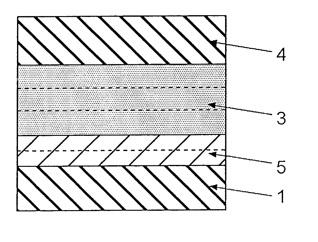
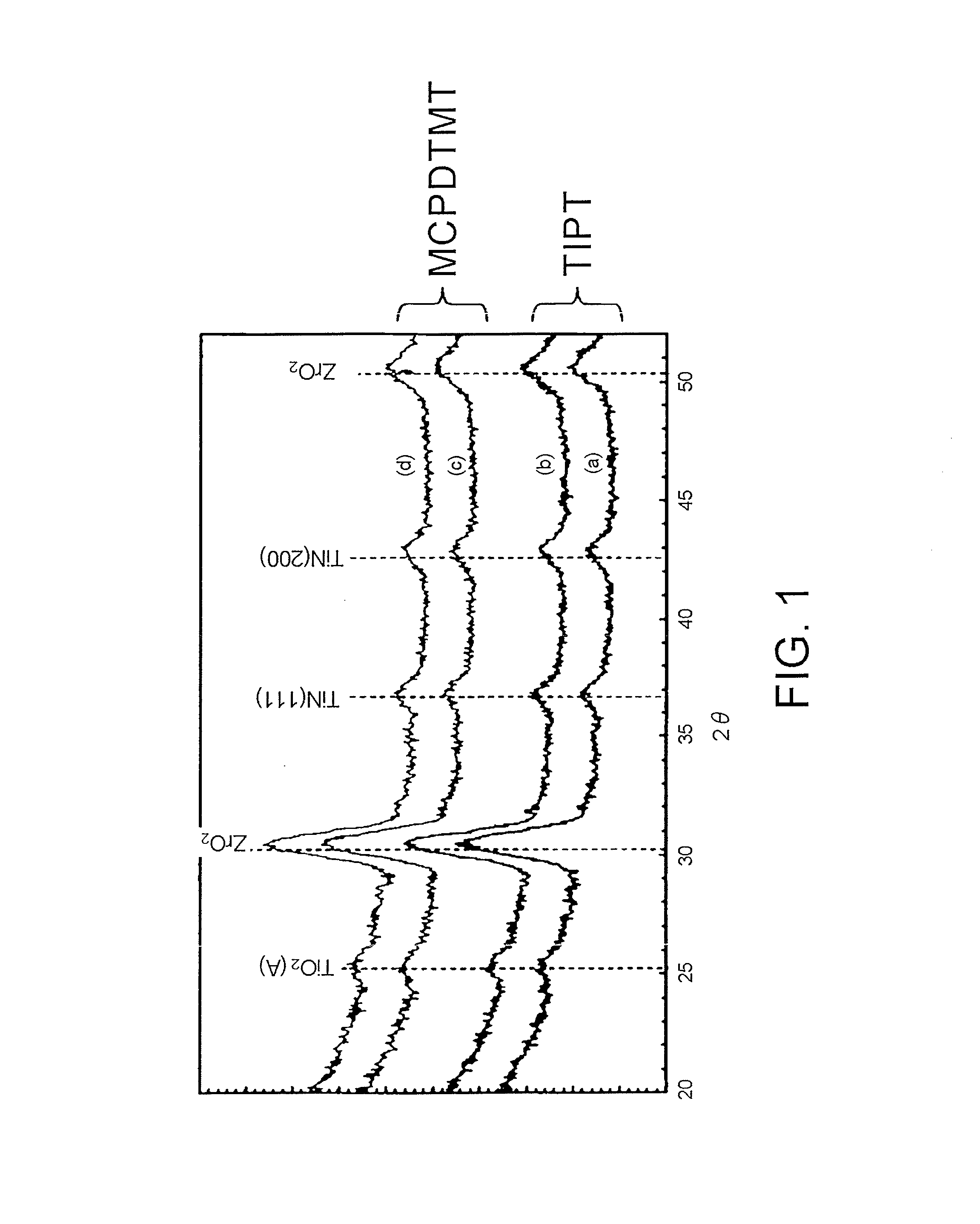
[0013]At first, the inventors were investigating an insulation film for a capacitor that has a multilayer structure of zirconium oxide (ZrO2) and titanium oxide (TiO2) (also referred to as a TZ structure). In the process of investigating this structure, the inventors found that a TiO2 film having a rutile crystalline structure can be formed without requiring high-temperature annealing when the TiO2 film is formed on a ZrO2 film under specific conditions.
[0016]According to an embodiment of the invention, it is possible to easily produce a titanium oxide film having a rutile crystalline structure at a low temperature, which was difficult to form in the related art.
[0017]In addition, it is possible to provide a semiconductor device having a capacitor that also has excellent leakage current characteristics by optimizing the thickness of the zirconium oxide film in the base.

Problems solved by technology

However, in the semiconductor process, it is difficult to perform annealing at a high temperature in order to protect semiconductor devices, such as a transistor, from adverse effects due to the progress of the miniaturization.
In consideration of application to capacitors, the annealing performed at a high temperature causes the surface of the electrode to be oxidized, thereby causing problems such as increased resistance and decreased adherence, when a metal film, particularly, a titanium nitride (TiN) film for general use is used as a lower electrode.
Therefore, in spite of the intention to produce the rutile phase crystal, the annealing at such a high temperature cannot be performed
In addition, if forming the TiO2 film in a place that has a three-dimensional structure, such as a capacitor of a DRAM device; it would be difficult to uniformly introduce Ar ions via ion radiation.
However, since the material of the lower electrode is limited to Ru, it is difficult to produce a capacitor having better performance by changing the material of the electrode.
In addition, even after every possible attempt was made to an annealing method, it was difficult to produce a TiO2 film that has only rutile phase crystals.

Method used


Image

  • Method of forming titanium oxide film having rutile crystalline structure
  • Method of forming titanium oxide film having rutile crystalline structure
  • Method of forming titanium oxide film having rutile crystalline structure

Examples


experimental example 1

[0029]First, in consideration of application to a capacitor, a TiN film having a thickness of 10 nm was formed as a lower electrode on a substrate, and then a ZrO film was formed thereon. The formation of the ZrO film was performed by repeating process steps a desired number of times, the process steps including (1) introducing a Zr source into a reaction chamber and causing the Zr source to be adsorbed on the surface of the TiN film, (2) discharging the remaining amount of the Zr source that was not adsorbed by a purge gas, such as N2 or Ar, from the reaction chamber, (3) oxidizing the Zr source using a reaction gas such as O3, and (4) purging the remaining amount of the reaction gas that has not reacted. Here, the ZrO film was formed at a thickness of 6 nm. The formed ZrO film was a crystalline film.

[0030]In sequence, a TiO film was formed on the resultant ZrO film by an ALD method. The formation of the TiO film was performed by repeating process steps a desired number of times, t...

experimental example 2

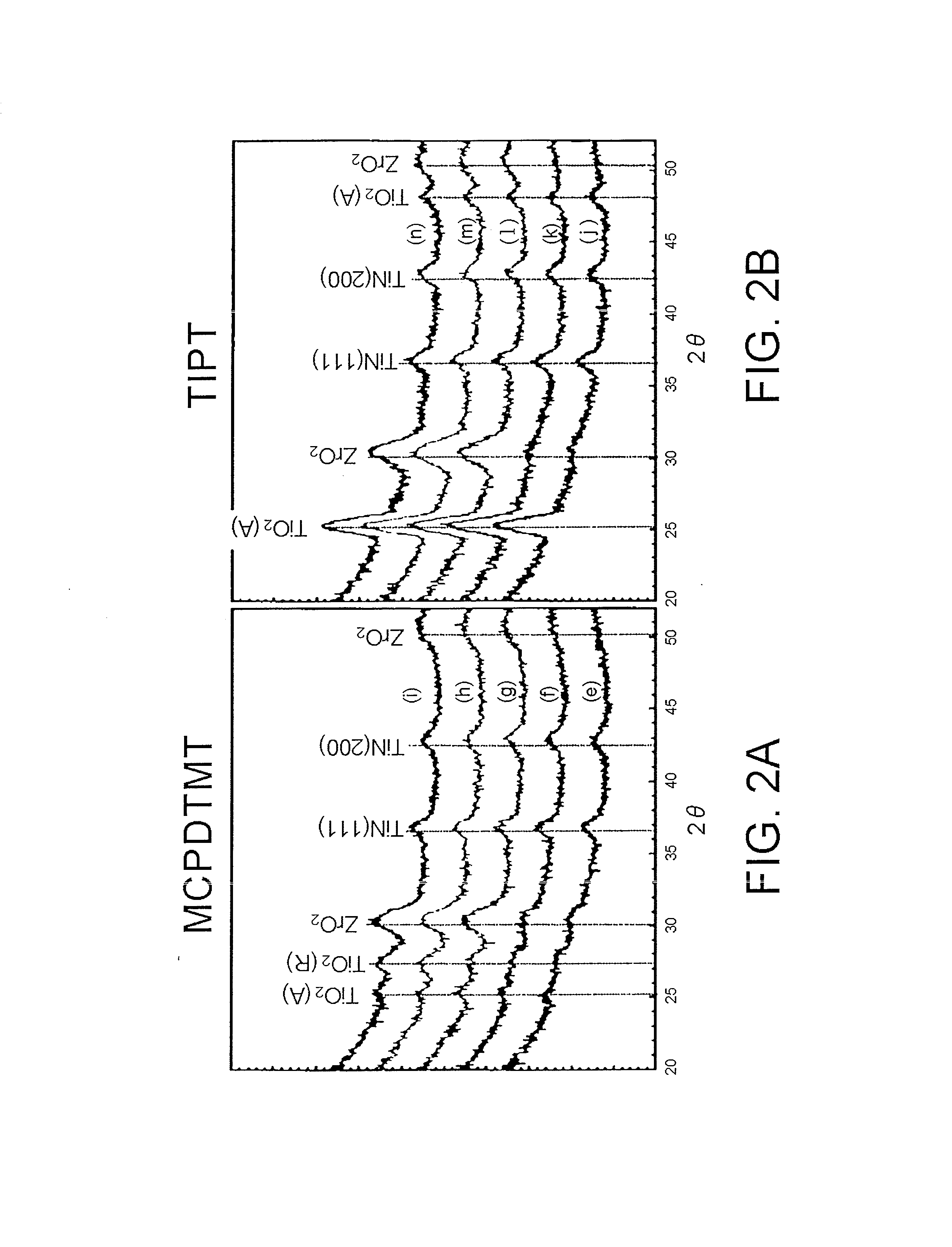
[0033]The formation of a TiO film on a ZrO film was performed in the same way as in Experimental Example 1 by changing the thickness of the ZrO film to 4 nm. Likewise, the results of performing X-ray diffraction were presented in FIG. 2. Here, annealing was performed under 4 temperature conditions, including 280° C., 300° C., 400° C. and 600° C. The annealing was performed in an oxidizing atmosphere at respective temperatures for 10 minutes. In FIG. 2A and FIG. 2B, FIG. 2A in the left presents the results when MCPDTMT was used as a Ti precursor, (e) as depo, (f) annealing at 280° C., (g) annealing at 300° C., (h) annealing at 400° C., and (i) annealing at 600° C., and FIG. 2B in the right presents the results when TIPT was used as a Ti precursor, (j) as depo, (k) annealing at 280° C., (l) annealing at 300° C., (m) annealing at 400° C., and (n) annealing at 600° C.

[0034]In the result (e) as depo using the MCPDTMT, only the peak of TiN of the lower electrode was observed, but no peak ...

experimental example 3

[0036]Next, it was verified whether or not a TiO film formed using MCPDTMT, in which the formation of the rutile crystalline structure was identified, can be used as a dielectric film for a capacitor by changing the thickness of a base ZrO film. In the experiment, the thickness of the TiO film was fixed to 8 nm, and the thickness of the ZrO film was varied up to 7 nm. The results obtained by measuring the relative permittivity of TiO films that were formed after being annealed at 600° C. are presented in FIG. 3. At thicknesses of the ZrO film ranging from 0.1 nm to 4 nm, high-permittivity TiO films were produced since the rutile phase was obtained. When the thickness of the ZrO film exceeds 4 nm, the anatase crystalline structure appeared, thereby lowering the relative permittivity. When the TiO film is directly formed on the TiN film (the thickness of the ZrO film is 0 nm), the anatase crystalline structure also appeared, thereby lowering the relative permittivity.

[0037]In sequence...


PUM

PropertyMeasurementUnit
temperatureaaaaaaaaaa
thicknessaaaaaaaaaa
thicknessaaaaaaaaaa

Abstract

The invention provides a method of forming a titanium oxide film having a rutile crystalline structure that has high permittivity. The titanium oxide film having a rutile crystalline structure is produced by forming an amorphous titanium oxide film on an amorphous zirconium oxide film using methyl cyclopentadienyl tris(dimethylamino)titanium as a titanium precursor by an ALD method, and crystallizing the amorphous titanium oxide film by annealing at a temperature of 300° C. or higher.

Description

BACKGROUND OF THE INVENTION[0001]1. Field of the Invention[0002]The present invention relates to a method of forming a titanium oxide (TiO2) film having a rutile crystalline structure, and more particularly, to a method of forming a film, which can be formed at a temperature of 700° C. or less, and also has excellent leakage current characteristics as a high-permittivity insulating film that is used in a capacitor.[0003]2. Related Art[0004]As the miniaturization of semiconductor devices such as dynamic random access memory (DRAM), a high-permittivity insulating film that is used in a capacitor is required.[0005]Titanium oxide (TiO2) can be regarded as an insulating material having high permittivity. In TiO2, two phases, i.e., an anatase phase and a rutile phase, are present as well-known crystalline structures. The anatase phase is a low-temperature phase that can be easily formed at a relatively low temperature, and the crystal of the anatase phase has a low relative permittivity t...

Claims


Application Information

Patent Timeline
Patent Type & Authority Applications(United States)
IPC IPC(8): H01G13/00H01L21/02
CPCH01L27/10817H01L27/10852H01L27/10894H01L28/40H01L21/02356H01L21/02186H01L21/0228H01L21/02304H01L28/91H10B12/318H10B12/033H10B12/09
Inventor KIYOMURA, TAKAKAZUHIROTA, TOSHIYUKIMOROZUMI, YUICHIROHISHIYA, SHINGO
Owner ELPIDA MEMORY INC
Learn More