Method for reprocessing semiconductor substrate, method for manufacturing reprocessed semiconductor substrate, and method for manufacturing SOI substrate

a technology of semiconductor substrate and manufacturing method, which is applied in the direction of semiconductor/solid-state device manufacturing, basic electric elements, electric devices, etc., can solve the problems of insufficient security of reprocessing and using bond substrates, and affecting the reprocessing treatment effect of semiconductor substrates. , the amount of loss of semiconductor substrate due to removal by polishing or the like in reprocessing treatment of semiconductor substrates can be reduced

Inactive Publication Date: 2012-12-27
SEMICON ENERGY LAB CO LTD
View PDF4 Cites 6 Cited by
  • Summary
  • Abstract
  • Description
  • Claims
  • Application Information

AI Technical Summary

Benefits of technology

[0021]According to an embodiment of the disclosed invention in this specification, a damaged semiconductor region can be selectively removed with respect to a non-damaged semiconductor region or a semiconductor region which is less damaged. Accordingly, the amount of loss of the semiconductor substrate due to removal by polishing or the like in reprocessing treatment of the semiconductor substrate can be reduced, and the number of times of reprocessing and using the semiconductor substrate can be increased.
[0022]Further, when a reprocessed semiconductor substrate is manufactured by the above method for reprocessing a semiconductor substrate, the productivity of the semiconductor substrate in the reprocessing treatment can be improved. Accordingly, cost for manufacturing the reprocessed semiconductor substrate can be reduced.
[0023]Furthermore, when an SOI substrate is manufactured using the above reprocessed semiconductor substrate, cost for manufacturing the SOI substrate can be reduced.

Problems solved by technology

This projection becomes a problem in a stage of reprocessing treatment of the bond substrate.
However, in order to remove the projection by polishing the surface through CMP treatment and reprocess the bond substrate as a novel bond substrate, the substrate has to be removed part of the substrate, which has a thickness of about 10 μm in the thickness direction, so that there is a problem in that the number of times of reprocessing and using the bond substrate cannot be sufficiently secured.

Method used


Image

  • Method for reprocessing semiconductor substrate, method for manufacturing reprocessed semiconductor substrate, and method for manufacturing SOI substrate
  • Method for reprocessing semiconductor substrate, method for manufacturing reprocessed semiconductor substrate, and method for manufacturing SOI substrate
  • Method for reprocessing semiconductor substrate, method for manufacturing reprocessed semiconductor substrate, and method for manufacturing SOI substrate

Examples


embodiment 1

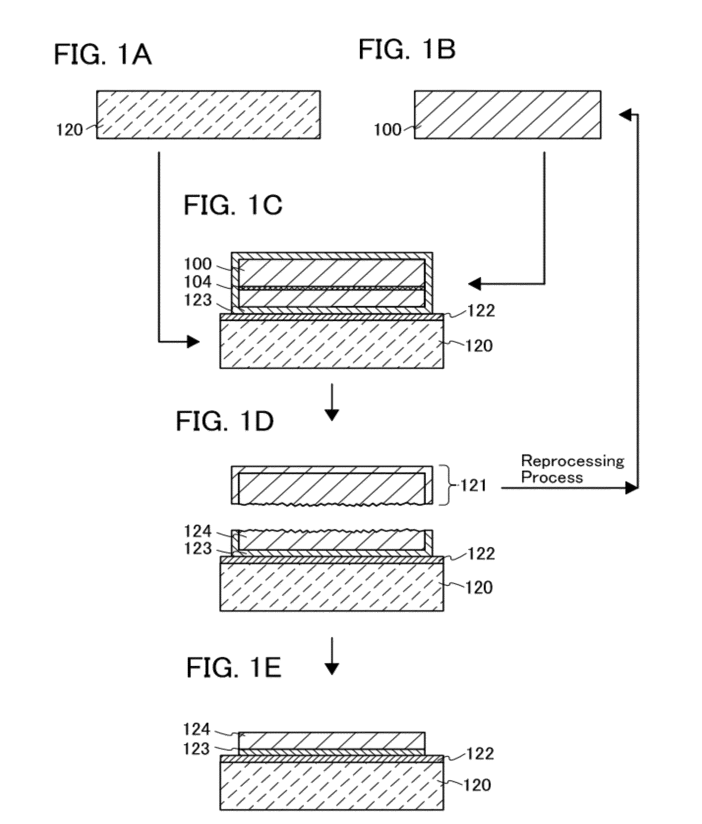
[0034]In this embodiment, an example of a method for manufacturing an SOI substrate and an example of a method for reprocessing a semiconductor substrate which is used for manufacturing the SOI substrate will be described with reference to FIGS. 1A to 1E and FIGS. 2A to 2D.

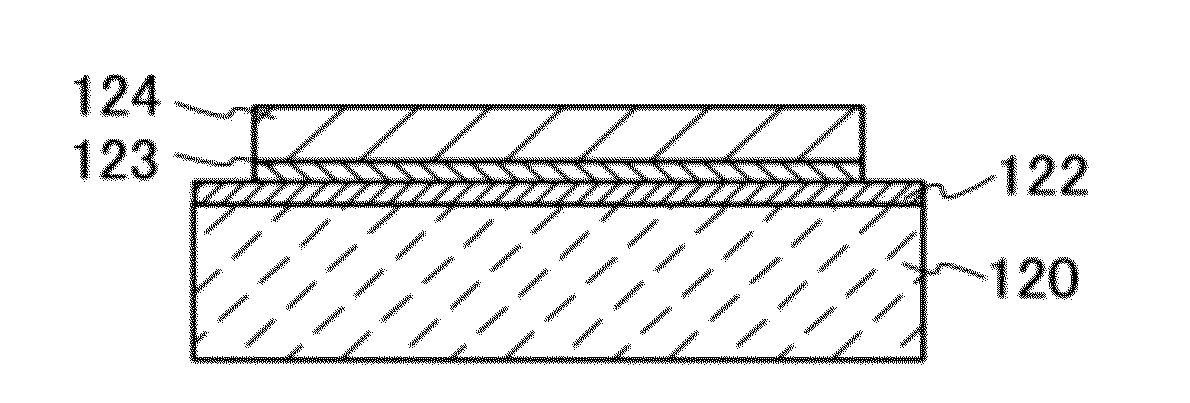
[0035]A process for manufacturing an SOI substrate is described with reference to FIGS. 1A to 1E. First, a base substrate 120 and a bond substrate are prepared (see FIGS. 1A and 1B).

[0036]As the base substrate 120, a substrate made of an insulator can be used. For example, variety of glass substrates used in the electronics industry, such as an aluminosilicate glass substrate, an aluminoborosilicate glass substrate, or a barium borosilicate glass substrate; a quartz substrate; a ceramic substrate, or a sapphire substrate can be given. Note that when the above glass substrate contains a large amount of boron oxide (B2O3), the heat resistance of glass is improved; and when it contains a larger amount of barium oxide...

embodiment 2

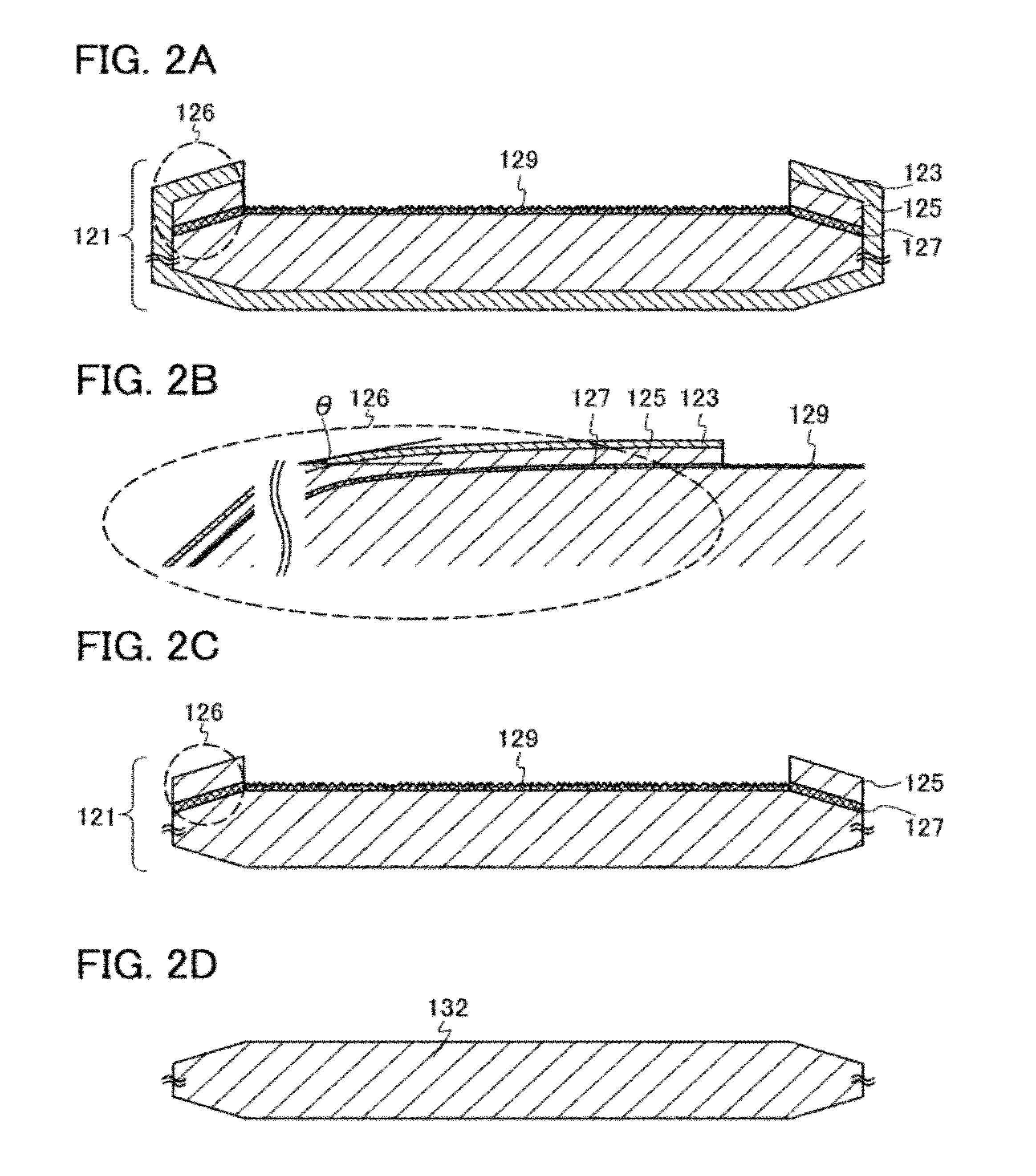
[0088]In a method for manufacturing an SOI substrate of this embodiment, an SOI substrate is manufactured by bonding a semiconductor layer separated from a semiconductor substrate which is a bond substrate to a base substrate. The semiconductor substrate from which the semiconductor layer has been separated is subjected to reprocessing treatment and reused as a bond substrate. An example of a method for manufacturing the SOI substrate of this embodiment will be described below with reference to FIGS. 3A to 3C, FIGS. 4A to 4C, and a manufacturing process chart of an SOI substrate of FIG. 5.

[0089]First, a process of forming an embrittlement region 104 in a semiconductor substrate 100 to prepare for bonding with a base substrate 120 is described. This process relates to treatment for the semiconductor substrate 100 and corresponds to Process A in FIG. 5.

[0090]First, the semiconductor substrate 100 is prepared (see FIG. 3A and the step A-1 in FIG. 5). As the semiconductor substrate 100,...

embodiment 3

[0158]In this embodiment, the case where an SOI substrate is manufactured using a silicon substrate or the like with high heat resistance as a base substrate will be described. Note that a method described in this embodiment is common to the above embodiment in many points. Therefore, different points will be mainly described in this embodiment. Drawings will not be particularly shown in this embodiment because drawings of this embodiment are in common with those of the above embodiment.

[0159]In a semiconductor substrate that is used as a bond substrate, an insulating layer and an embrittlement region are formed (corresponding to Process A in FIG. 5). Treatment and the like for the semiconductor substrate, which includes the formation of the insulating layer and the embrittlement region, are similar to those in the above embodiment. Therefore, description in the above embodiment may be referred to for such treatment and the like.

[0160]In this embodiment, a substrate with high heat r...


PUM


Abstract

A method suitable to reprocess a semiconductor substrate is provided. A semiconductor substrate in which a projection including a damaged semiconductor region and an insulating layer is provided in a peripheral portion of the semiconductor substrate is subjected to etching treatment for removing the insulating layer and to etching treatment for removing the damaged semiconductor region selectively with a non-damaged semiconductor region left using a mixed solution including nitric acid, a substance dissolving a semiconductor material included in the semiconductor substrate and oxidized by the nitric acid, a substance controlling a speed of oxidation of the semiconductor material and a speed of dissolution of the oxidized semiconductor material, and nitrous acid, in which the concentration of the nitrous acid is higher than or equal to 10 mg/l and lower than or equal to 1000 mg/l. Through these steps, the semiconductor substrate is reprocessed.

Description

BACKGROUND OF THE INVENTION[0001]1. Field of the Invention[0002]The invention to be disclosed relates to a method for reprocessing a semiconductor substrate. In addition, the invention to be disclosed relates to a method for manufacturing a reprocessed semiconductor substrate with the use of the method for reprocessing a semiconductor substrate, and relates to a method for manufacturing an SOI (silicon on insulator) substrate.[0003]2. Description of the Related Art[0004]In recent years, instead of a bulk silicon wafer, integrated circuits using an SOI (silicon on insulator) substrate that includes a thin single crystal silicon layer formed on an insulating surface have been developed. The characteristics of the thin single crystal silicon layer formed on the insulating surface make it possible to completely separate transistors formed in the integrated circuit from each other. Further, since fully-depleted transistors can be formed, a semiconductor integrated circuit with high added...

Claims


Application Information

Patent Timeline
Patent Type & Authority Applications(United States)
IPC IPC(8): H01L21/762H01L21/302
CPCH01L21/02238H01L21/02255H01L21/30604H01L21/76254H01L21/31111H01L21/02032H01L21/3105
Inventor HANAOKA, KAZUYAKIMURA, SHUNSUKE
Owner SEMICON ENERGY LAB CO LTD
Why Eureka
Try Eureka