

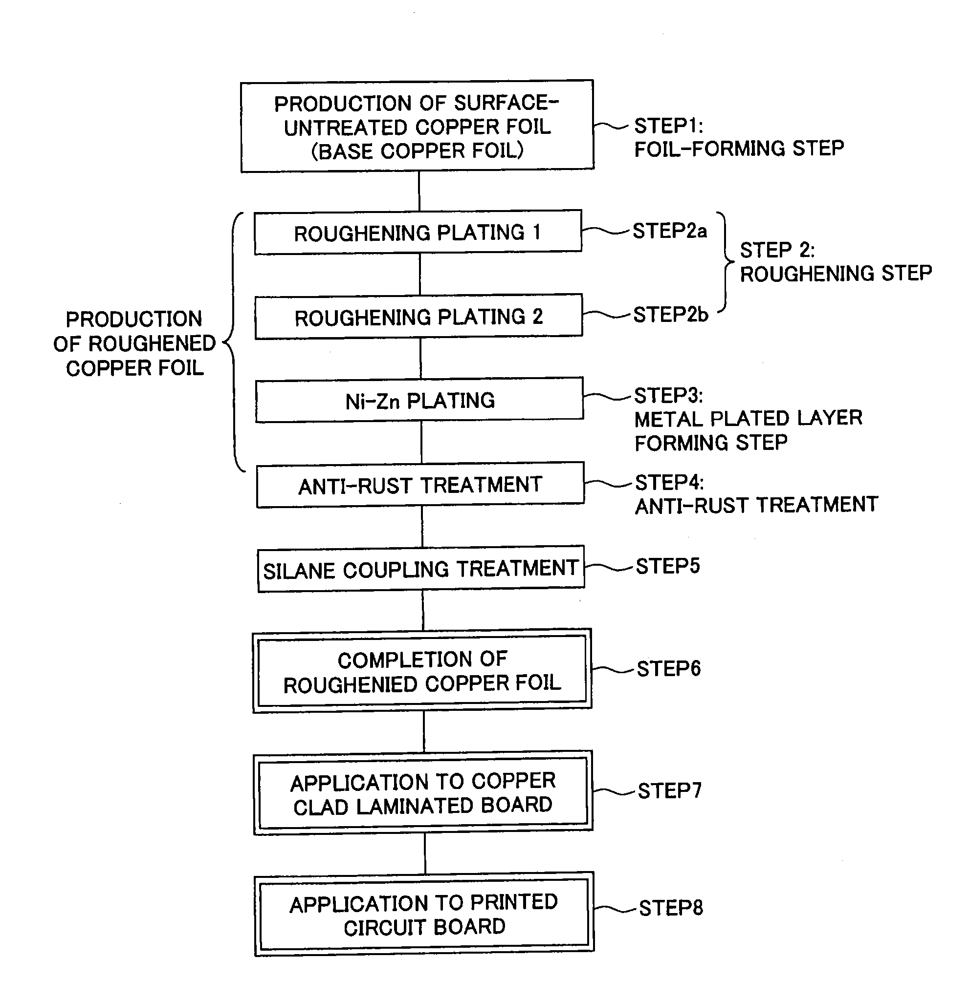
Surface-treated copper foil, method for producing same, and copper clad laminated board
a surface-treated copper foil and laminated board technology, which is applied in the field of copper foil and a method for producing the same and to a copper-clad laminated board, can solve the problems of lowering the productivity of the circuit board, lowering the cost of surface-treated copper foil, and not yet providing surface-treated copper foil to meet these characteristics. , to achieve the effect of soft etching
- Summary
- Abstract
- Description
- Claims
- Application Information
AI Technical Summary
Benefits of technology
Problems solved by technology
Method used
Image

Examples
synthesis example 1
[0112]A reactor vessel provided with a thermocouple and a stirrer and capable of introduction of nitrogen was charged with N,N-dimethylacetamide (DMAc). In this reactor vessel, 2,2- bis[4-(4-aminophenoxy)phenyl]propane (BAPP) was dissolved while stirring in the vessel. Next, pyromellitic dianhydride (PMDA) in equivalent mol to the diamine ingredient was added. After that, stirring was continued for about 3 hours to perform the polymerization reaction, whereby a resin solution of polyamide acid having a solid concentration of 15 wt % and solution viscosity of 3000 cps was obtained. A polyimide film was prepared by using the polyamide acid “a” and was measured for its glass transition temperature. As a result, it was 280° C., and the result of measurement of the linear expansion coefficient was 55×10−6 [1 / K].
synthesis example 2
[0113]A reactor vessel provided with a thermocouple and a stirrer and capable of introduction of nitrogen was charged with DMAc. In this reactor vessel, 2,2′-dimethyl-4,4′-diaminobiphenyl (m-TB) was dissolved while stirring in the vessel. Next, pyromellitic dianhydride (PMDA) in equivalent mol to the diamine ingredient was added. After that, stirring was continued for about 3 hours to perform the polymerization reaction, whereby a resin solution of polyamide acid “b” having a solid concentration of 15 wt %, and solution viscosity of 20000 cps was obtained. A polyimide film was prepared by using the polyamide acid “b” and was measured for its linear expansion coefficient. As a result, it was 13×10−6 [1 / K].
Preparation of Test Pieces
[0114]The above polyamide acid resin was applied to the produced untreated copper foils by the methods shown in the examples to obtain test pieces.
[0115]Measuring means, measurement conditions
[0116](1) Measurement of Deposition Amounts of Metal
[0117]Analysi...
example 1
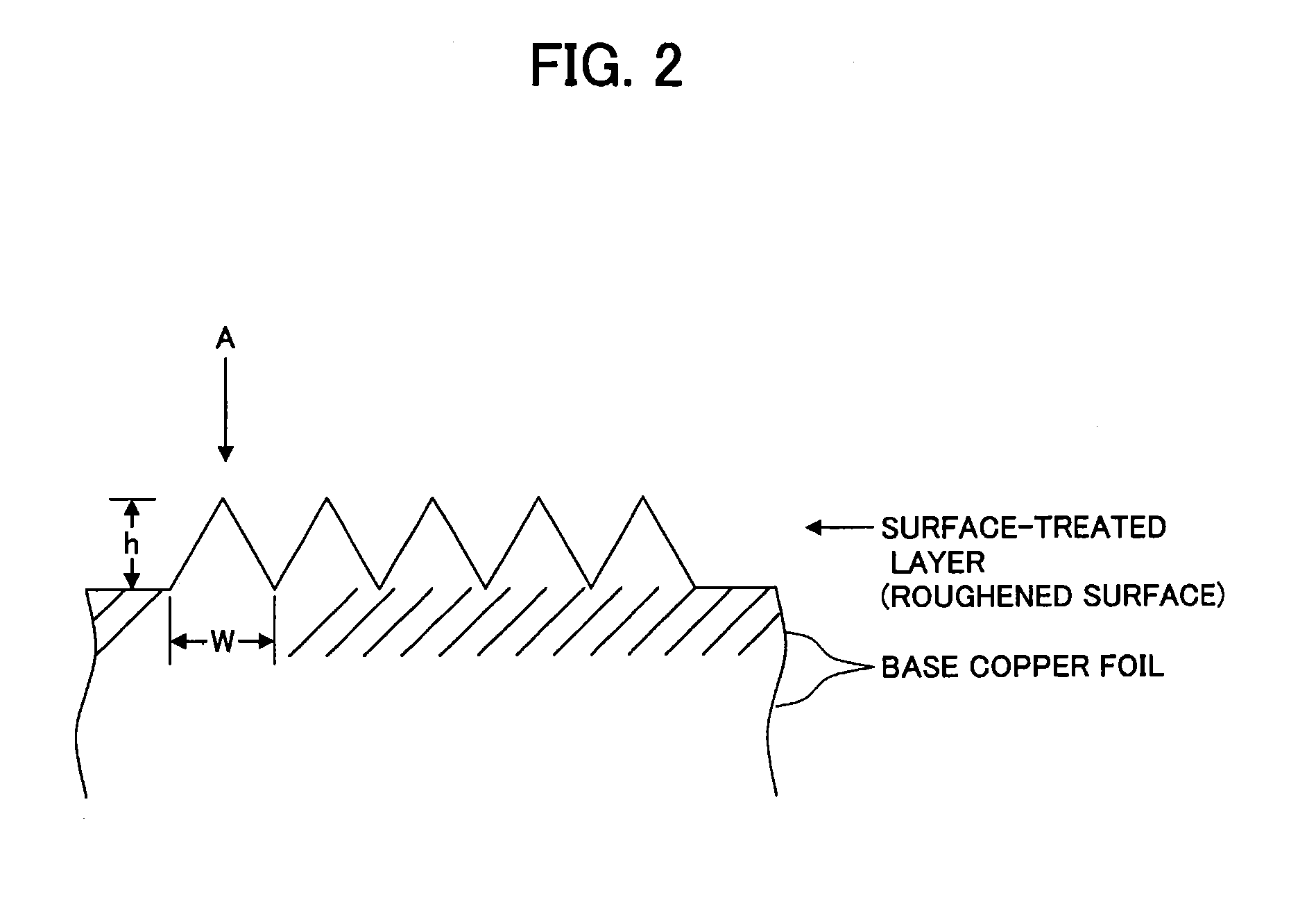
[0147]To the surface of a base copper foil (untreated electrolytic copper foil) having surface roughnesses (Ra) of 0.08 μm and (Rz) of 0.58 μm, microroughening giving an increased amount of roughening after roughness formation of 0.03 μm in (Ra) and 0.15 μm in (Rz) was applied. The aspect ratio of roughening at this time was 1.4, and the surface area ratio was 3.7.
[0148]On this surface, a surface treated layer made by Ni—Zn alloy and chromate treated layer were formed, and a 3-aminopropyltrimethoxysilane treated layer was formed. The amount of nickel of the copper foil surface at that time was 0.91 mg / dm2, and the amount of zinc was 0.17 mg / dm2.
[0149]On this copper foil, a thermoplastic polyimide layer was formed by using the polyamide acid “a” produced in the above Synthesis Example 1 so that the thickness after hardening became 2 μm, a low thermal expansion resin layer was formed on that by using the polyamide acid “b” produced in the above Synthesis Example 2 so that the thicknes...
PUM
| Property | Measurement | Unit |
|---|---|---|
| surface roughness Rz | aaaaa | aaaaa |
| surface roughness Ra | aaaaa | aaaaa |
| surface roughness Ra | aaaaa | aaaaa |
Abstract
Description
Claims
Application Information