Methods to form substrates for optical sensing by surface enhanced raman spectroscopy (SERS) and substrates formed by the methods

a technology of substrates, which is applied in the field of methods of forming substrates for optical sensing by surface enhanced raman spectroscopy, and to substrates formed by the methods, can solve the problems of limited commercialization of sers techniques, amplification of signal intensity, and non-uniform enhancement of state-of-the-art sers substrates

Inactive Publication Date: 2013-02-21
AGENCY FOR SCI TECH & RES
View PDF1 Cites 42 Cited by
  • Summary
  • Abstract
  • Description
  • Claims
  • Application Information

AI Technical Summary

Benefits of technology

[0055]An advantage of a substrate formed by such methods is that no lithography or electron beam lithography is involved, thus providing a simple, inexpensive and quick technique to achieve a highly sensitive and spatially uniform SERS signal, e.g., for biomedical applications. A treatment step, such as wet etching or dry etching, may be used to treat the polymeric nanoparticles that are attached to the surface of the support to vary the template size. In so doing, the resolution of the template, such as the size of the polymeric nanoparticles and the interparticle distance between the polymeric nanoparticles, may be customized in a simple manner. Using such methods, highly uniform, precise and well-defined metallic arrays of sub-5 nm separations may be achieved. Furthermore, such methods to form the substrate may be advantageous in that no linkers are required to attach the metallic nanoparticles to the polymeric nanoparticles attached on the support. Instead, the metallic nanoparticles may directly attach to the polymeric nanoparticles by electrostatic attraction, thereby eliminating extra process steps. In further embodiments, the treatment step may be used to remove the polymeric template. In so doing, a metal nanoarray substrate of arrays of metallic nanoparticles clusters (termed herein as “super-clusters”) on a support may be formed.

Problems solved by technology

Coherent interference of their electromagnetic (EM) field may lead to a red-shift in coupled plasmon resonance, and may result in amplification of the signal intensity.
Commercialization of SERS techniques has thus far been limited due to a number of challenges.
However, state-of-the-art SERS substrates often suffer from non-uniform enhancement across their surfaces, as existing substrate fabrication processes aim to enhance signals for single-molecule detection, and as a result, produce hotspot congregations that are highly localized.
Other substrate-related issues include inconsistent signal enhancement at different points on the same substrate, batch-to-batch variations in signal, the complexity of fabrication, cost effectiveness of mass production, the stability of the substrate, and the difficulty of detecting wide range of analytes.
Even though techniques such as electron beam lithography have been used to produce precise and well-defined metallic arrays on substrates to overcome such reproducibility issues, these techniques are expensive and time consuming.
Furthermore, these techniques lack the ability to fabricate arrays over macroscopic areas, thereby posing problems in terms of scalability.
State-of-the-art techniques are also usually not versatile, in that they are not able to be used on the surfaces of some types of material, and are not able to be used on non-planar surfaces.
However, inconsistencies due to the lack of reproducibility of the self-assembly process, low signal enhancement in SERS, and the possibility of random multilayer formation on the fiber tip, resulting in opaque fiber faucets, are issues compromising the applicability of this technique.
Even though techniques such as UV lithography and nanoimprinting have also been used, these techniques still suffer from limitations relating to signal enhancement, as well as ease of fabrication.
However, this technique is cumbersome and cannot be translated into biological environment, since nanoparticle solutions cannot survive the harsh ionic conditions of biological media.

Method used


Image

  • Methods to form substrates for optical sensing by surface enhanced raman spectroscopy (SERS) and substrates formed by the methods
  • Methods to form substrates for optical sensing by surface enhanced raman spectroscopy (SERS) and substrates formed by the methods
  • Methods to form substrates for optical sensing by surface enhanced raman spectroscopy (SERS) and substrates formed by the methods

Examples


example 1

Materials

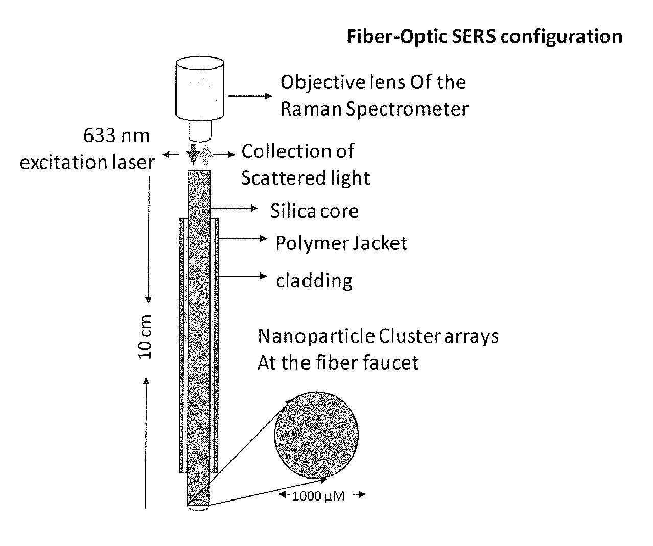
[0116]Polystyrene-block-poly(2-vinylpyridine) (PS-b-PVP) (57000-b-57000 g / mol) was purchased from Polymer Source Inc. (Montreal, Canada). Silicon and quartz substrates were purchased from Silicon Valley Microelectronics (SVM, CA, USA). (3-Aminopropyl) trimethoxysilane (APTMS, 95%) and crystal violet (CV, FW: 407.99) were purchased from Sigma-Aldrich. Hexane, ethanol (both analytical grade), hydrochloric acid (HCl, 37%), nitric acid (HNO3, 65%), sulphuric acid (H2SO4, 95-97%) and hydrogen peroxide (H2O2) were purchased from Merck. Optical fibers with 1000 μm diameter and 0.37 numerical aperture having a hard polymer cladding with silica core was purchased from Thorlabs (BFH37-1000, fiber ID F10-056T).

example 2

Characterization Methods

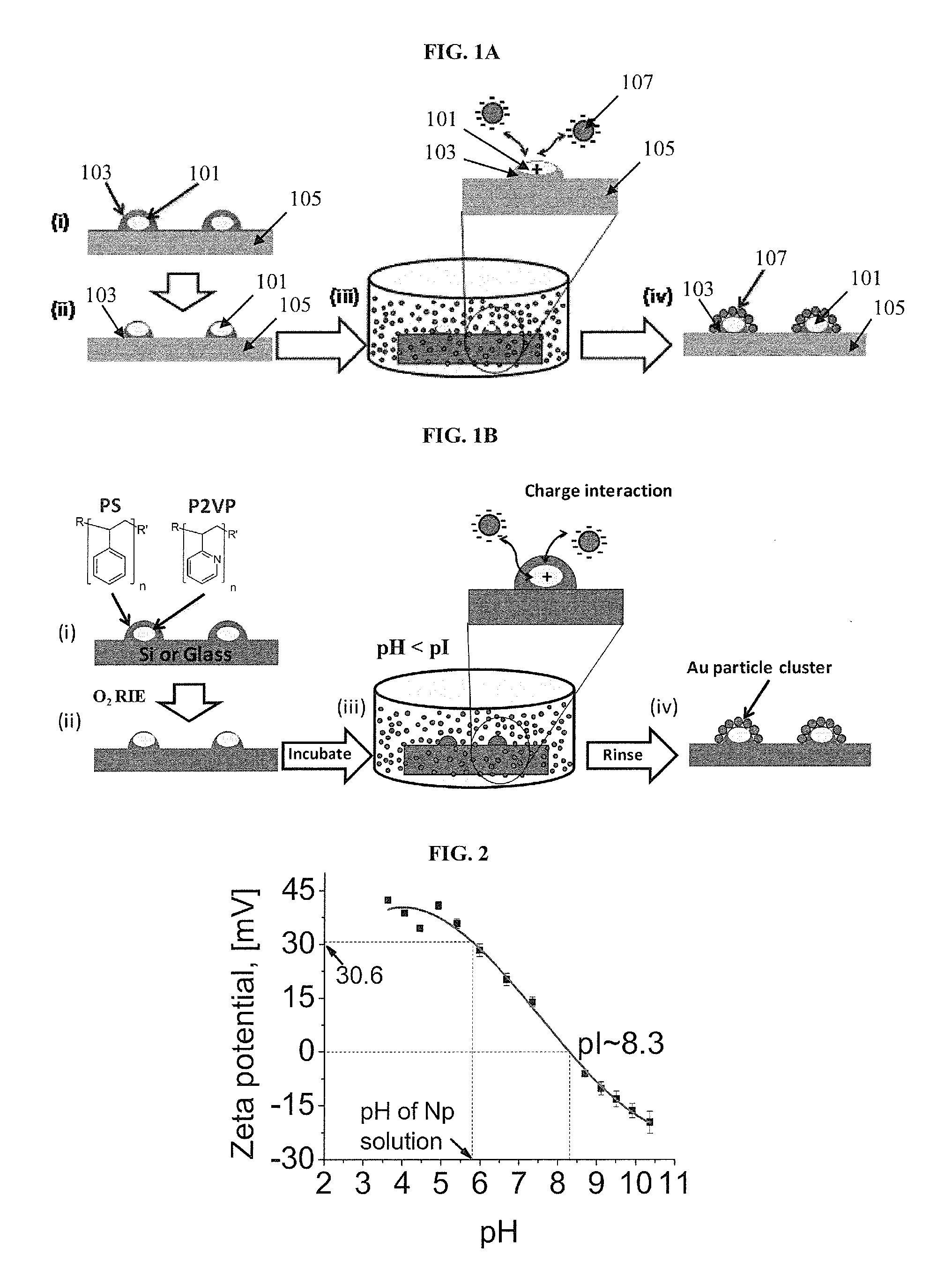
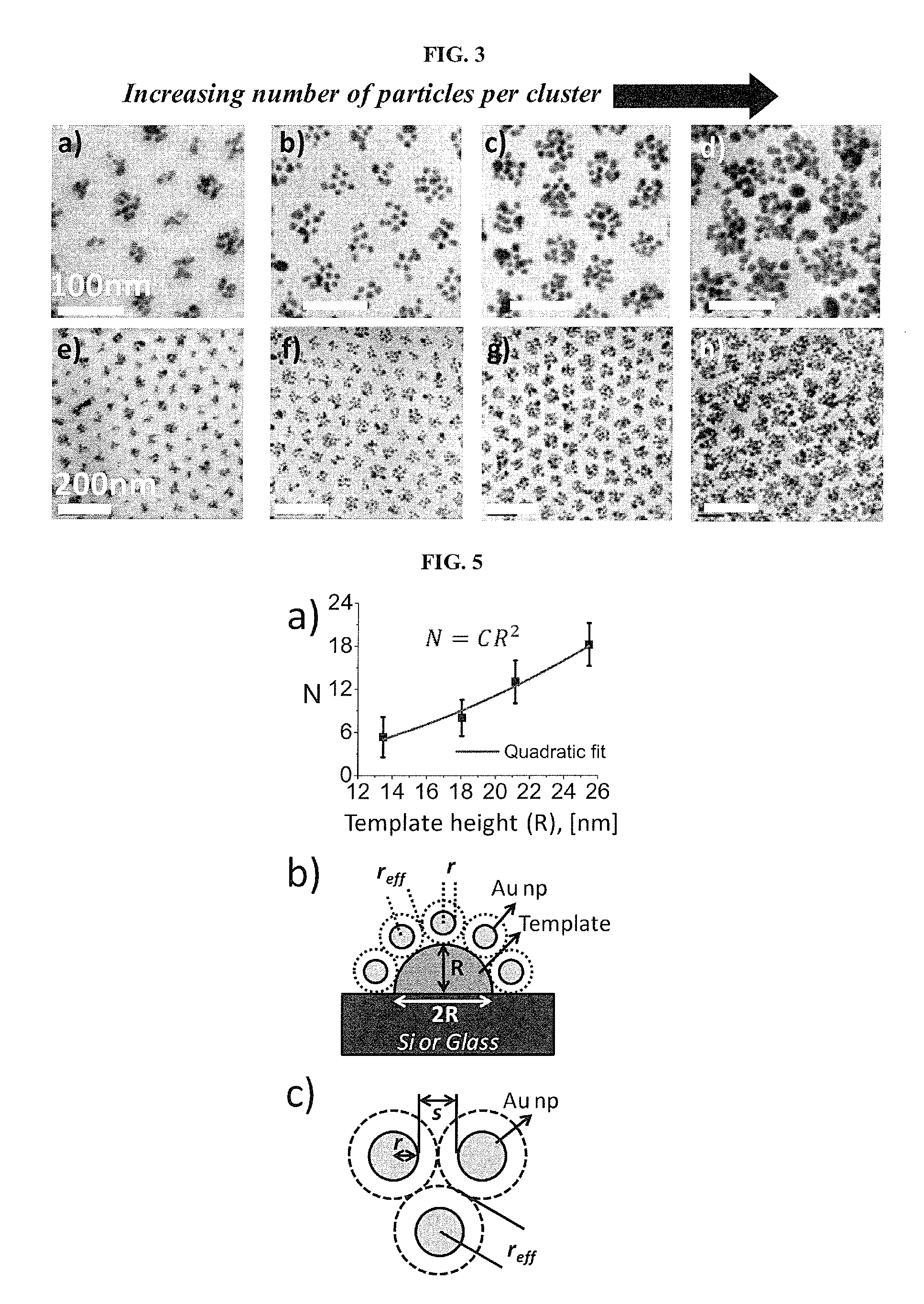
[0117]The zeta potential of the surface coated with micelle arrays was determined by streaming potential measurements using SurPASS electro-kinetic analyzer (Anton Par, VA, USA). Electrophoretic measurements on gold nanoparticles were carried out using Zetasizer Nano ZS (Malvern, Worcestershire, UK). The samples used for the measurement measured 20 mm×10 mm. The templates, nanoparticle clusters, and the unpatterned gold nanoparticles were characterized with tapping mode AFM (Nanoscope IV Multimode AFM, Veeco Instruments Inc., NY, USA), SEM (FESEM 6700F, JEOL, Tokyo, Japan) and TEM (Philips CM300) operating at 300 kV. The extinction spectra of the gold nanoparticles assembly on glass substrates were recorded using CRAIC Spectrophotometer (CRAIC Technologies, CA, USA). An unpolarized light source was used with measurement spot areas of 77 μm×77 μm.

example 3

Preparation of Fiber Substrates

[0118]The fibers were cut into 10 cm pieces by a cleaver. The jacket and cladding were stripped to a length of approximately 1.5 cm from each end. Both ends were then polished using alumina polishing sheets (1 μm) using standard techniques. The polished ends were then washed for about 2 to 3 minutes with a jet of water and sonicated in ethanol for 10 minutes and dried.


PUM

PropertyMeasurementUnit
inter-particle distanceaaaaaaaaaa

Abstract

A method of manufacturing a substrate is provided. The method comprises, in some aspects, a) providing a support; b) forming a template by attaching a plurality of polymeric nanoparticles some or all having a core-shell structure to the support, wherein the core comprises a first polymer and the shell comprises a second polymer; and c) forming the metal nanoarray substrate by attaching a plurality of metallic nanoparticles to at least some of the polymeric nanoparticles of the template. A biosensor comprising a substrate manufactured by the method, and a method for the detection of an analyte in a sample by surface enhanced Raman spectroscopy (SERS) is also provided.

Description

CROSS-REFERENCE TO RELATED APPLICATIONS[0001]This application makes reference to and claims the benefit of priority of an application for “A Method For Fabricating Metal Nanoarrays On Optical Fiber Faucet For High-Performance SERS Based Remote Sensing Of Molecular Analytes, Using Directed Self-Assembly Gold Nanoparticles” filed on Aug. 19, 2011, with the Intellectual Property Office of Singapore, and there duly assigned serial number 201106015-9. The content of said application filed on Aug. 19, 2011, is incorporated herein by reference in its entirety for all purposes.TECHNICAL FIELD[0002]Some aspects of the invention relate to methods of forming substrates for optical sensing by surface enhanced Raman spectroscopy (SERS), and to substrates formed by the methods.BACKGROUND[0003]Vibrational spectroscopic techniques, such as infra-red (IR), normal Raman Spectroscopy and Surface Enhanced Raman Spectroscopy (SERS), have been considered for analyte detection. Of these, SERS has evolved ...

Claims


Application Information

Patent Timeline
Patent Type & Authority Applications(United States)
IPC IPC(8): C40B30/00C40B50/18C40B40/14B82Y15/00B82Y30/00
CPCG01N33/54346G01N33/54373B81B2201/0214B81C1/00206G01N21/658
Inventor YAP, FUNG LINGKRISHNAMOORTHY, SIVASHANKARTHONIYOT, PRAVEENSURESH, VIGNESHDINDA, SANGHAMITRA
Owner AGENCY FOR SCI TECH & RES
Why Eureka
Try Eureka