

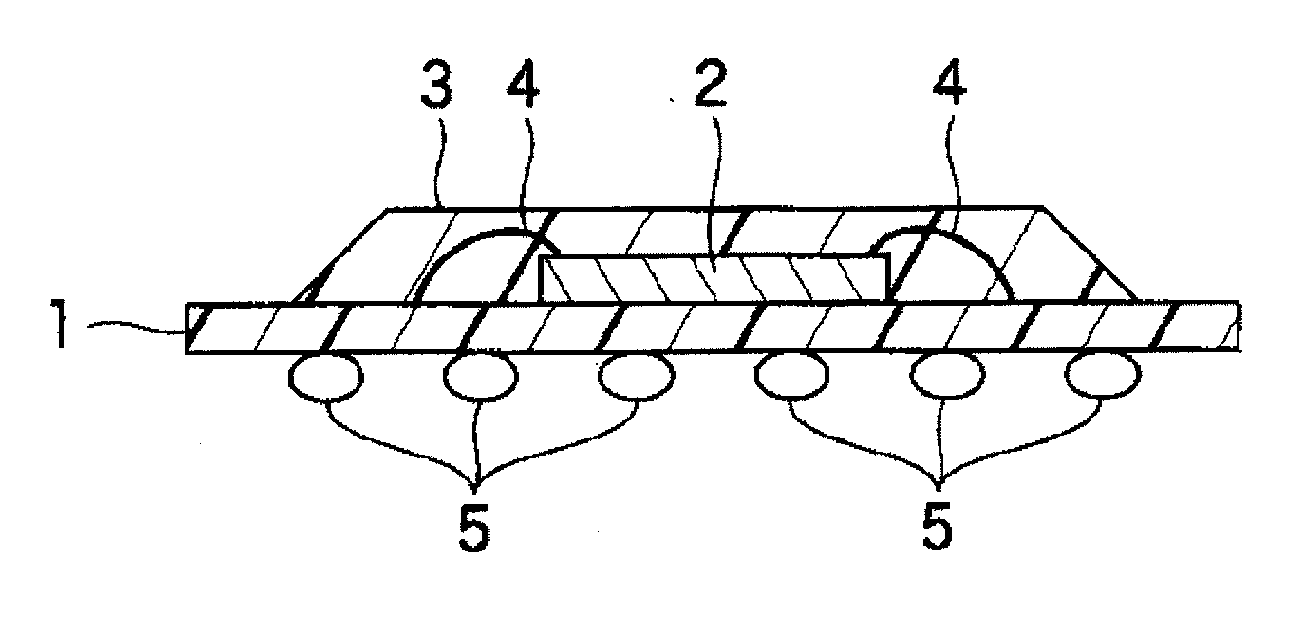
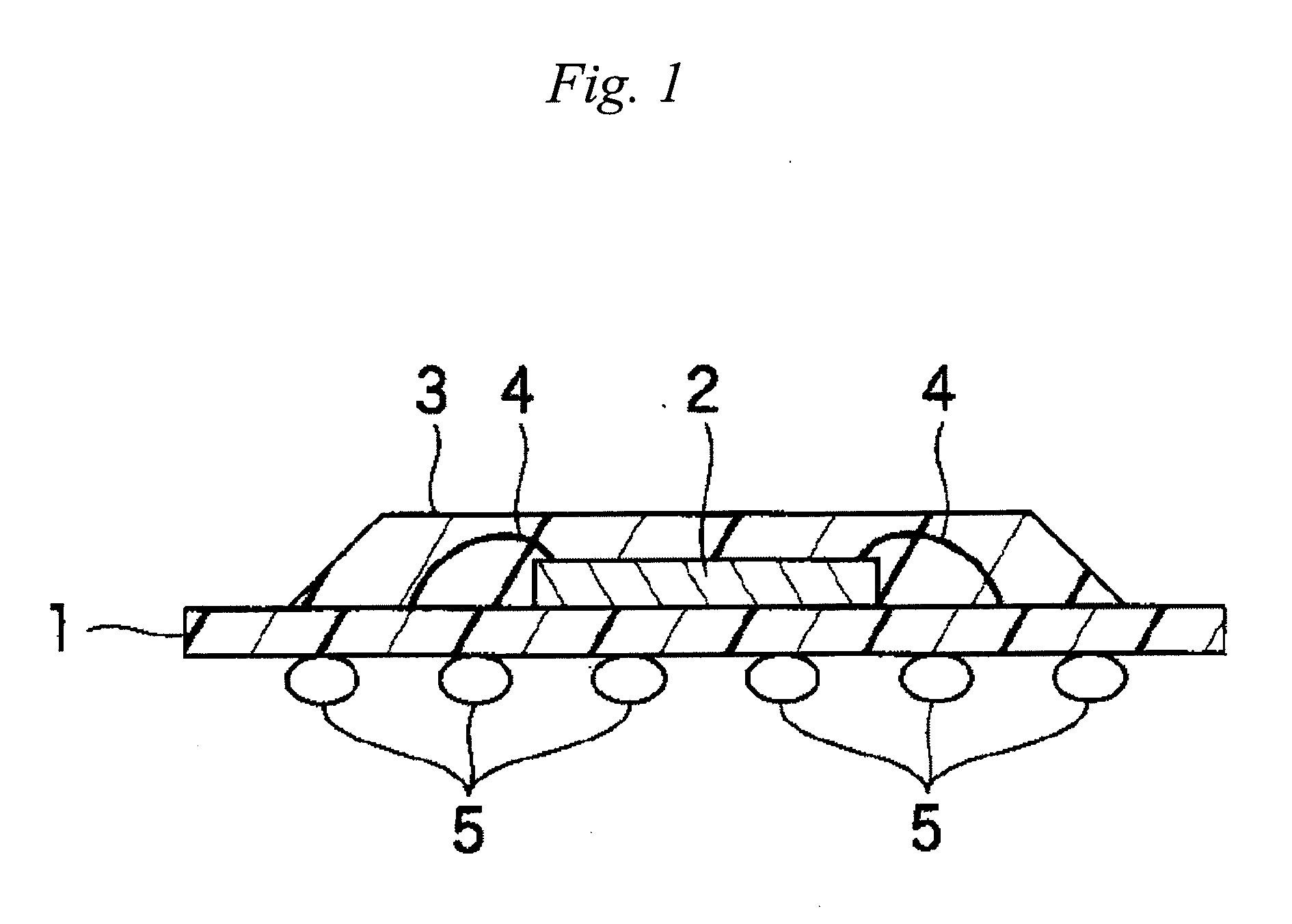
Epoxy resin composition for semiconductor encapsulation and semiconductor device using the same
a technology of epoxy resin and semiconductor encapsulation, which is applied in the direction of solid-state devices, coatings, basic electric elements, etc., can solve the problems of limiting the method of increasing the glass transition temperature of the cured resin, deteriorating flame retardancy, etc., and achieves excellent powder blocking properties, reduces the dependency of the warpage temperature, and suppresses the warpage of the package
- Summary
- Abstract
- Description
- Claims
- Application Information
AI Technical Summary
Benefits of technology
Problems solved by technology
Method used
Image

Examples
examples
[0067]The present invention is described below by reference to the following Examples and Comparative Examples, but the invention is not construed as being limited to those Examples.
[0068]First, the following components were prepared.
Epoxy Resin
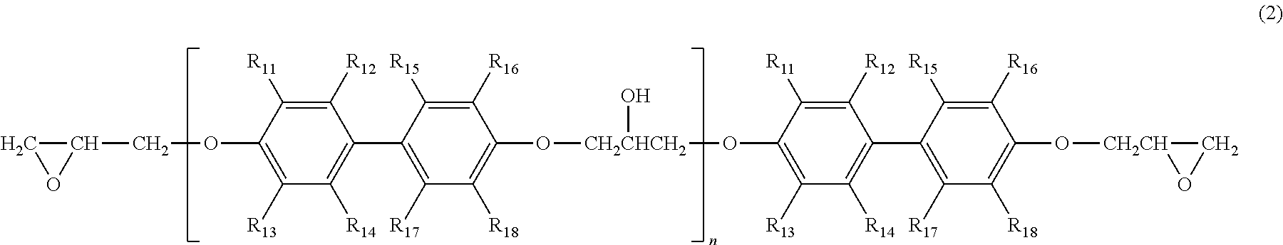
[0069]Biphenyl type epoxy resin represented by the formula (2) in which R11 to R18 are a methyl group, and n is 0 (epoxy equivalent: 192, melting point: 105° C.)
Phenol Resin b1
[0070]Biphenyl aralkyl type phenol resin (hydroxyl equivalent: 203, softening point: 65° C.)
Phenol Resin b2
[0071]Phenol novolak resin (hydroxyl equivalent: 104, softening point: 60° C.)
Phenol Resin b3
[0072]Triphenylmethane type phenol resin (hydroxyl equivalent: 97, softening point: 111° C.)
Curing Accelerator
[0073]2-Phenyl-4-methyl-5-hydroxymethylimidazole
Ethylene Glycol Type Compound d1 (Example)
[0074]Monoethylene glycol (number average molecular weight: 62; in the formula (1), n=1, R1=OH and R2=H)
Ethylene Glycol Type Compound d2 (Example)
[0075]Diethylene glycol (numbe...
PUM
| Property | Measurement | Unit |
|---|---|---|
| weight | aaaaa | aaaaa |
| moldability | aaaaa | aaaaa |
| shrinkage | aaaaa | aaaaa |
Abstract
Description
Claims
Application Information