Neutron detector and method of making
a neutron detector and detector technology, applied in the field of neutron detectors, can solve the problems of limiting the potential sensitivity of these detectors, he-3 is uneconomic for many neutron detection applications, and the former normally has a substantially lower neutron detection sensitivity, so as to reduce voltage and power requirements, effectively discriminate neutrons, and improve signal characteristics
- Summary
- Abstract
- Description
- Claims
- Application Information
AI Technical Summary
Benefits of technology
Problems solved by technology
Method used
Image
Examples
example 1
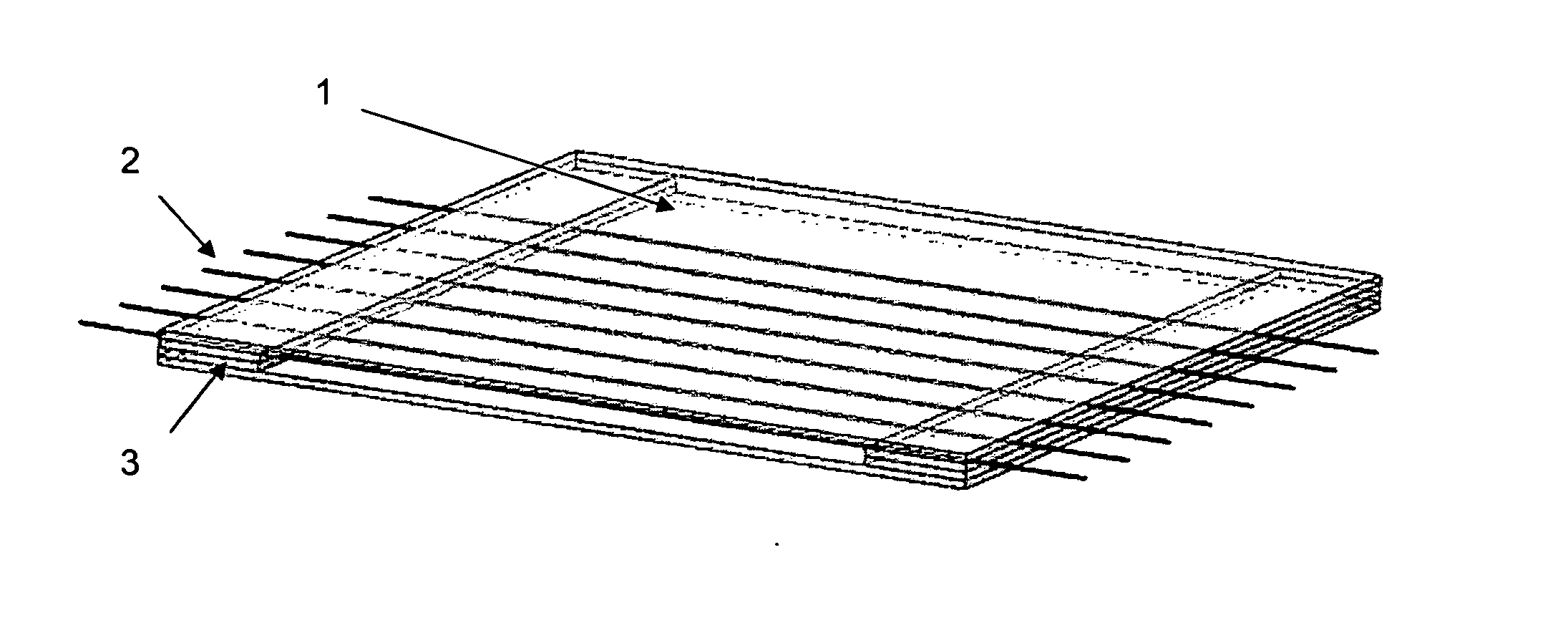
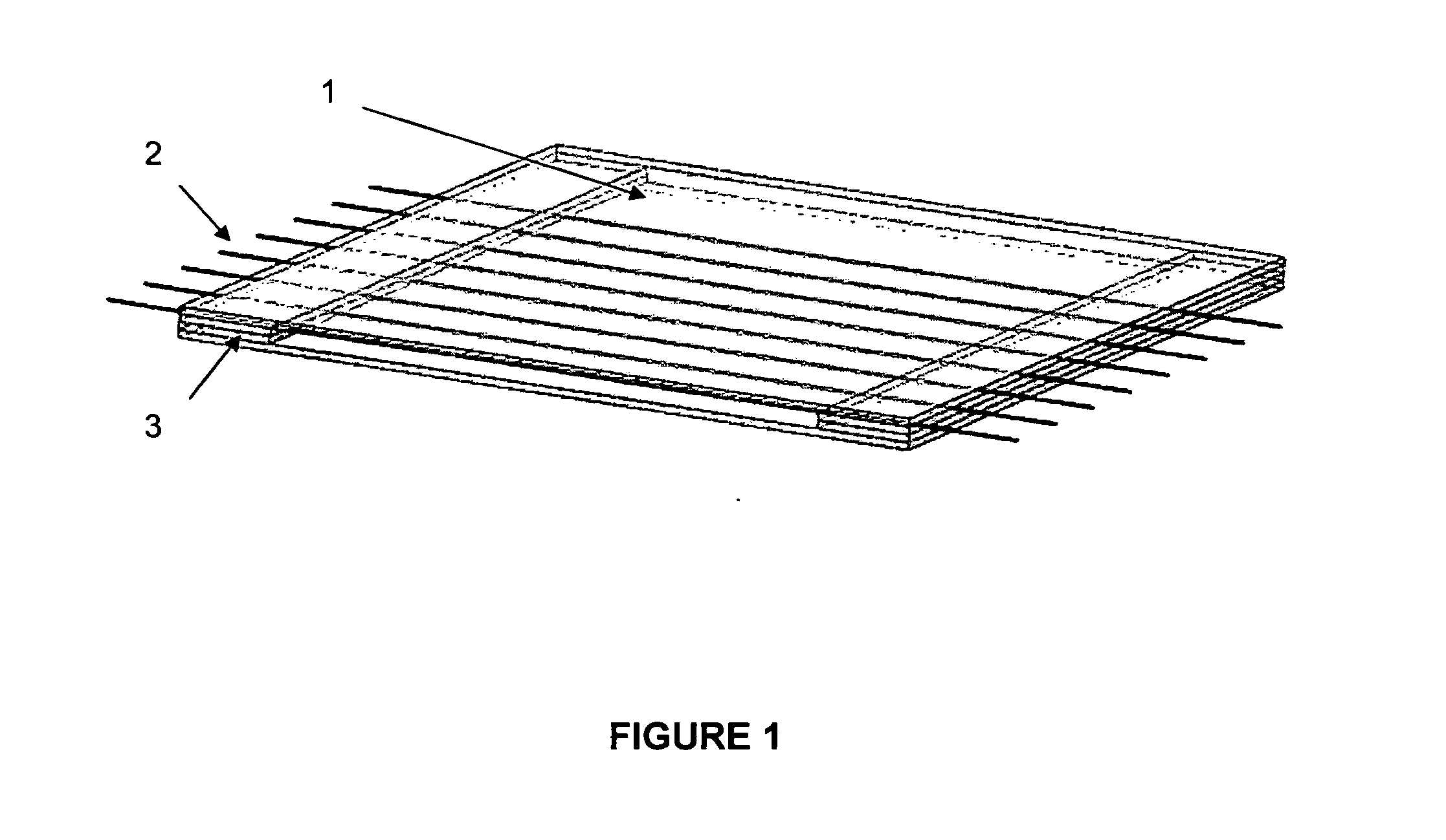
[0095]Flat Stacked Detector: A 35 cm long, 5 cm wide, copper sheet of 50 micrometers thickness was coated with boron layer on both sides. The boron layer consisted of B4C enriched with 96% B-10 with an average areal density of 0.14 mg / cm2. A set of Teflon sheets 0.5 mm thick×5.5 cm long×3.5 cm wide, were cut with four windows of 1.9 cm on a side, as shown in FIG. 7. Two Teflon sheets were applied against the copper sheet such that the Teflon sheets were centered on the width of the copper sheet. A 25 μm diameter conductive wire was woven around the two Teflon sheets such that the wire did not touch the copper sheet as shown in FIG. 8. A second set of Teflon sheets were then applied onto the first set of Teflon sheets such that the wire was sandwiched between two Teflon sheets on each side of the copper sheet. The copper sheet was then folded around the dielectric-anode sandwich once. This process was repeated four more times, creating a 2 cm thick structure comprising five layers of...
example 2
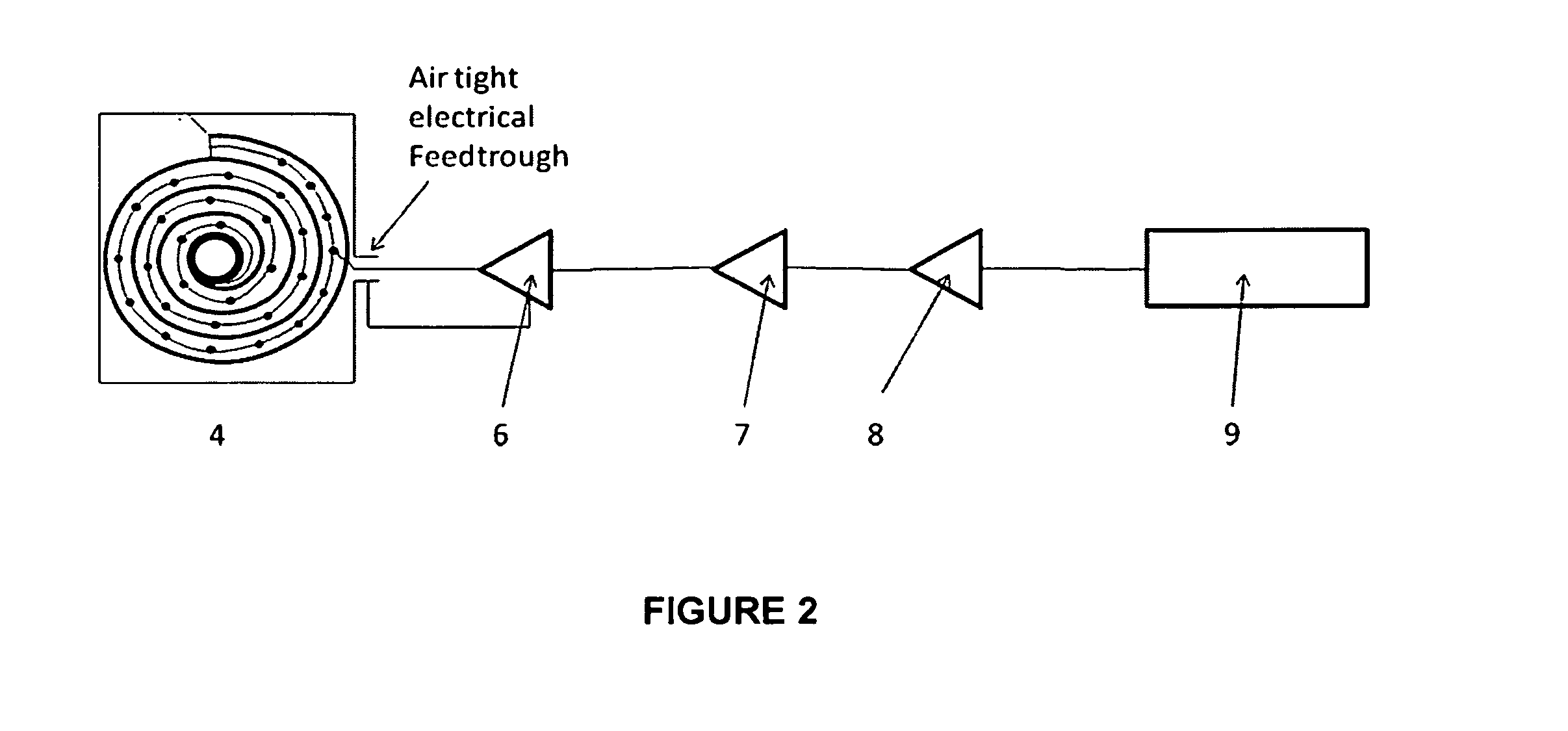
[0097]Cylindrical Detector with Single Copper Sheet in Spiral Configuration: A 0.05 mm thick copper sheet of 63 cm length and 15.2 cm width was coated on both sides with boron carbide isotopically enriched to 96% B-10. The average coating thickness was about 0.5 μm. The coating was applied to the copper sheet in strips of around 12 mm width with around 3 mm separation between the coated strips along the length of the sheet. The last 2.5 cm at one end of the copper sheet and the last 10 cm at the other end were left uncoated, enabling the uncoated portion of the copper sheet to constitute the outer surface of the detector when the detector is closed and sealed. Strips of Teflon 3 mm wide were prepared with adhesive on each side. Two strips 6 mm wide were prepared similarly and V-shaped notches were made on one side every 4 mm. A length of 1.6-cm diameter copper tubing was used as the substrate. The end of the copper sheet was rolled around the copper tube and maintained in place with...
example 3
[0099]Concentric Cylindrical Tubes: In a conceptual design validated by simulation, a central cylinder, having an outer diameter of 12 mm, is coated on its outer surface with a boron layer having a thickness of about 1 micrometer. A ring made of dielectric sheet-like material, having an inside diameter substantially equal to the outer diameter of the copper cylinder, such that it fits around said copper cylinder, and having a thickness of about 0.7 mm and a length of 6 mm is applied at each extremity of the cylinder in such a way that half of its length lies against the copper cylinder, and the other half extends beyond the copper cylinder. The outer edges of the dielectric rings are cut to create a series of notches spaced about every 4 mm and about 1 mm deep. A 0.025 mm conductive wire is woven from one ring to the other, hooking onto each ring via the small notches described above. The distance between each loop of wire is thus about 4 mm. A second set of rings is applied on the ...
PUM
 Abstract
Description
Claims
Application Information


