Silicon carbide substrate and method of manufacturing the same

a technology of silicon carbide and substrate, which is applied in the direction of polycrystalline material growth, crystal growth process, synthetic resin layered products, etc., can solve the problem of 0.01 cm sup>2 as the lower limit of the micropipe density, and achieve excellent performance and stable forming

Active Publication Date: 2013-03-21
SUMITOMO ELECTRIC IND LTD
View PDF0 Cites 34 Cited by
  • Summary
  • Abstract
  • Description
  • Claims
  • Application Information

AI Technical Summary

Benefits of technology

[0006]The present invention was made to solve such problems, and an object of the present invention is to provide a silicon carbide substrate capable of stably forming a device of excellent performance, and a method of manufacturing the same.
[0008]With these features, when an epitaxial layer made of silicon carbide is formed on a main surface of the silicon carbide substrate, the density of defects that affect the performance of a device including the epitaxial layer can be reliably reduced, thereby improving the device performance.
[0009]The width (e.g., diameter) of the silicon carbide substrate is set to not less than 100 mm, in order to lower the cost of manufacturing the device. The width of the silicon carbide substrate is preferably not less than 120 mm, and more preferably not less than 150 mm. The micropipe density is set to not more than 7 cm−2, in order to prevent a photoresist from reaching a back surface of the silicon carbide substrate during application of the photoresist in the process of manufacturing the device. The micropipe density is preferably not more than 5 cm−2, and more preferably not more than 3 cm−2. The lower limit of the micropipe density is 0.01 cm −2 due to manufacturing limitations and the like.
[0011]The basal plane dislocation density is set to not more than 1×104 cm−2, in order to improve long-term reliability of the device. The basal plane dislocation density is preferably not more than 5×105 cm−2, and more preferably not more than 3×105 cm−2. The lower limit of the basal plane dislocation density is 1×106 cm−2 due to manufacturing limitations and the like.
[0017]The present inventors have found that vibration applied to a processing container during growth of silicon carbide introduces defects resulting from the vibration into a grown silicon carbide layer. Specifically, when vibration is applied to a processing container, the shape of a surface of source powder placed in the processing container may vary due to the vibration, causing silicon carbide to be formed on the surface of a seed crystal substrate under growth conditions that are not optimal conditions. The vibration may also stir up part of the source powder in the processing container, causing the occurrence of defects in formed silicon carbide. In order to prevent the occurrence of these problems, it is effective to control the maximum values of the frequency and amplitude of vibration applied to the processing container as described above.
[0020]According to the present invention, a silicon carbide substrate with reduced defects which is capable of forming a device of excellent performance can be obtained.

Problems solved by technology

The lower limit of the micropipe density is 0.01 cm −2 due to manufacturing limitations and the like.

Method used


Image

  • Silicon carbide substrate and method of manufacturing the same
  • Silicon carbide substrate and method of manufacturing the same
  • Silicon carbide substrate and method of manufacturing the same

Examples


example

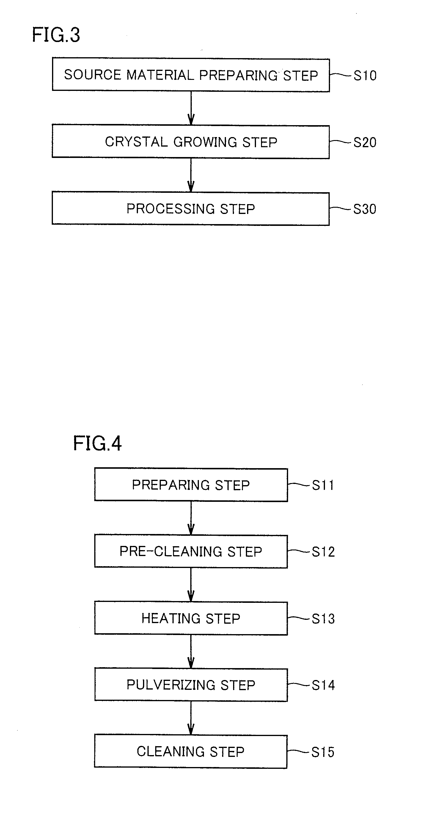
[0121]Samples of a silicon carbide substrate were fabricated in order to confirm the effect of the present invention.

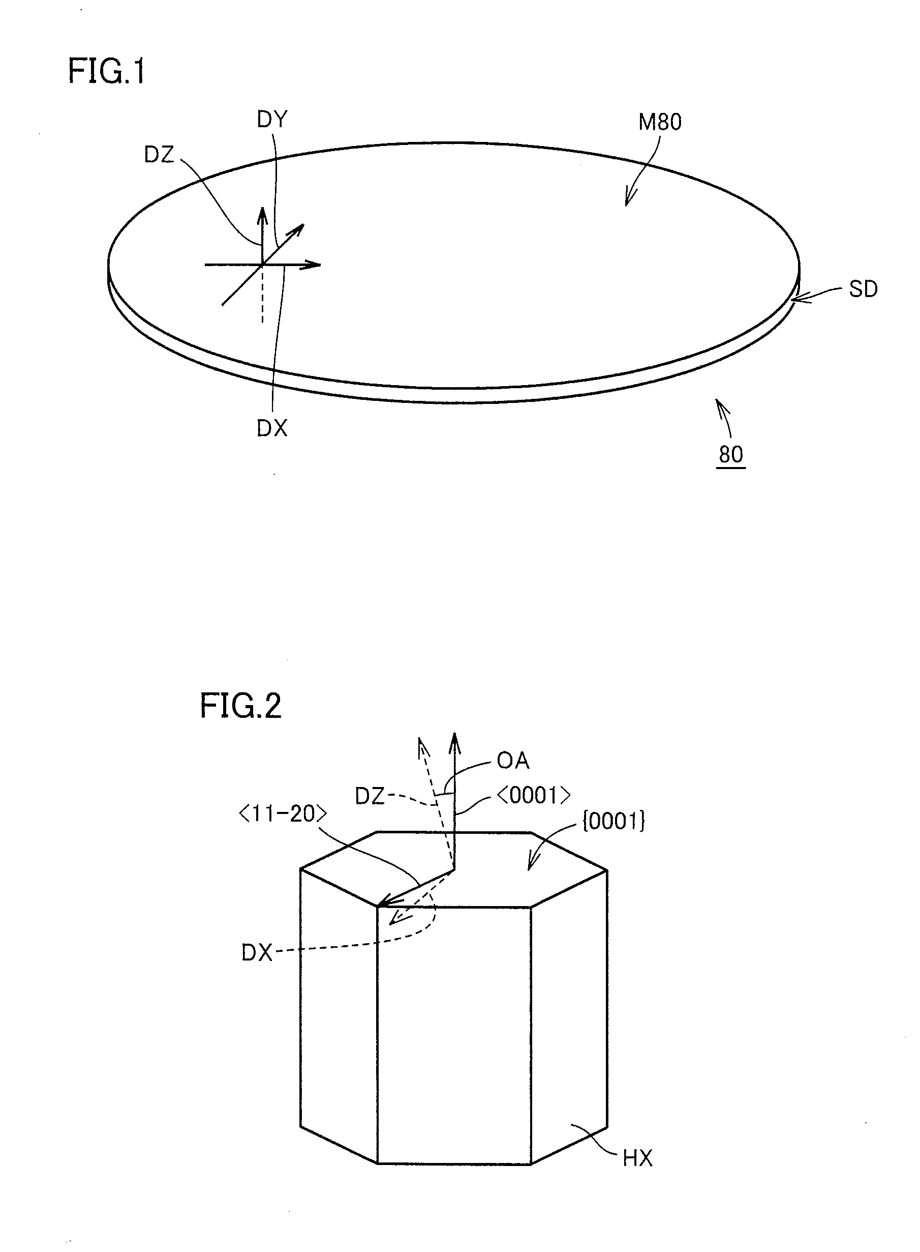
[0122](Preparation of Source Material) First, a plurality of small pieces of silicon having a diameter of not less than 1 mm and not more than 1 cm, and carbon powder having an average particle size of 200 μm were prepared. The small pieces of silicon were silicon chips having a purity of 99.999999999% used for withdrawing a silicon single crystal.

[0123]Next, 1541 g of the small pieces of silicon and 659 g of the carbon powder thus prepared were lightly kneaded, and the resultant mixture was charged into a graphite crucible. The graphite crucible used was heated in advance to 2300° C. in a high-frequency furnace under reduced pressure of 0.013 Pa of argon gas, and maintained for 14 hours.

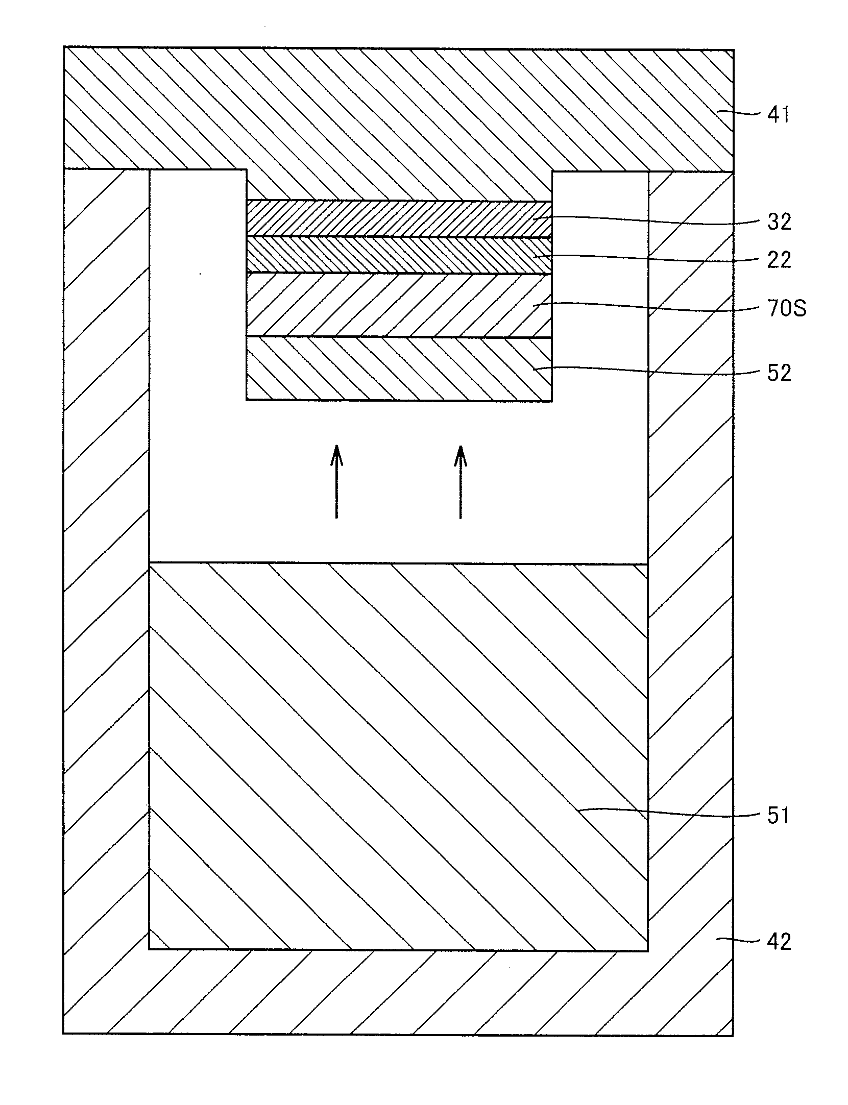
[0124]Next, the graphite crucible into which the mixture of the small pieces of silicon and carbon powder was charged was placed in an electric furnace, and was vacuumed until the pre...


PUM

PropertyMeasurementUnit
frequencyaaaaaaaaaa
thicknessaaaaaaaaaa
tensile strengthaaaaaaaaaa

Abstract

A silicon carbide substrate capable of stably forming a device of excellent performance, and a method of manufacturing the same are provided. A silicon carbide substrate is made of a single crystal of silicon carbide, and has a width of not less than 100 mm, a micropipe density of not more than 7 cm−2, a threading screw dislocation density of not more than 1×104 cm−2, a threading edge dislocation density of not more than 1×104 cm−2, a basal plane dislocation density of not more than 1×104 cm−2, a stacking fault density of not more than 0.1 cm−1, a conductive impurity concentration of not less than 1×1018 cm−2, a residual impurity concentration of not more than 1×1016 cm−2, and a secondary phase inclusion density of not more than 1 cm−3.

Description

BACKGROUND OF THE INVENTION[0001]1. Field of the Invention[0002]The present invention relates to silicon carbide substrates and methods of manufacturing the same, and more particularly to a silicon carbide substrate capable of forming a device of excellent performance, and a method of manufacturing the same.[0003]2. Description of the Background Art[0004]A silicon carbide substrate has been used to manufacture a semiconductor device in recent years. Silicon carbide has a wider band gap than silicon, which is a more common material. Thus, a semiconductor device including a silicon carbide substrate has advantages including high breakdown voltage, low on-resistance, and high resistance to performance degradation in a high temperature environment.[0005]It has been conventionally proposed to use a silicon carbide substrate having a reduced density of crystal defects, in order to realize a semiconductor device of excellent performance as described above. For example, U.S. Pat. No. 7,314,...

Claims


Application Information

Patent Timeline
Patent Type & Authority Applications(United States)
IPC IPC(8): C30B23/02C01B31/36
CPCC30B23/005C30B29/36C30B35/007H01L21/02631H01L21/02433H01L21/02529H01L21/02378C30B23/025
Inventor HARADA, SHINFUJIWARA, SHINSUKENISHIGUCHI, TARO
Owner SUMITOMO ELECTRIC IND LTD
Why Eureka
Try Eureka