Epitaxial substrate and method for manufacturing epitaxial substrate

a technology of epitaxial substrate and nitride, which is applied in the direction of semiconductor devices, electrical equipment, transistors, etc., can solve the problems of reducing reliability and cost, affecting the formation of good nitride, and difficult forming a good nitride film on a silicon substrate, etc., to achieve excellent surface flatness, excellent crystal quality, and excellent breakdown voltage properties

Inactive Publication Date: 2013-04-18
NGK INSULATORS LTD
View PDF4 Cites 10 Cited by
  • Summary
  • Abstract
  • Description
  • Claims
  • Application Information

AI Technical Summary

Benefits of technology

[0037]In the first to sixteenth aspects of the present invention, the compressive strain exists in the buffer layer. Accordingly, a tensile stress caused by a difference in a thermal expansion coefficient between silicon and a group-III nitride is cancelled by the compressive strain. Therefore, a crack-free epitaxial substrate having a small amount of warping and an excellent crystal quality can be obtained even when a silicon substrate is used as the base substrate.
[0038]Particularly, in the eighth, ninth, fourteenth, and fifteenth aspects, a crack-free epitaxial substrate having a small amount of warping and excellent breakdown voltage properties is achieved.
[0039]Particularly, in the tenth and sixteenth aspects, the buffer layer is provided on the base layer having a low dislocation and an excellent surface flatness. Accordingly, the buffer layer, the crystal layer, and the like, have good crystal quality. On the other hand, an accumulation of strain energy in the second base layer is suppressed. Therefore, the effect of canceling the tensile stress exerted by the compressive strain existing in the buffer layer is not hindered by any accumulation of strain energy in the base layer.

Problems solved by technology

The HEMT device and the HEMT-device substrate involve various problems including problems concerning improvement of the performance such as increasing the power density and efficiency, problems concerning improvement of the functionality such as a normally-off operation, fundamental problems concerning a high reliability and cost reduction, and the like.
However, it is known that forming a nitride film of good quality on a silicon substrate is very difficult as compared with a case of using a sapphire substrate or a SiC substrate, for the following reasons.
In other words, this is a factor that hinders the formation of a good nitride epitaxial film having a low dislocation density and a flat surface.
As a result, it is likely that cracking occurs in a film surface and large warping occurs in the substrate.
However, the resulting GaN film never has a better crystal quality as compared with a case of using SiC or sapphire for the base substrate.
Therefore, preparing an electronic device such as a HEMT using the conventional techniques involves problems of a low electron mobility, a leakage current during the off-time, and a low breakdown voltage.
Furthermore, in the method disclosed in the Patent Document 4, large convex warping is intentionally caused in the course of the device preparation.
This may cause cracking in the course of the device preparation, depending on conditions under which the layers are formed.

Method used


Image

  • Epitaxial substrate and method for manufacturing epitaxial substrate
  • Epitaxial substrate and method for manufacturing epitaxial substrate
  • Epitaxial substrate and method for manufacturing epitaxial substrate

Examples


example

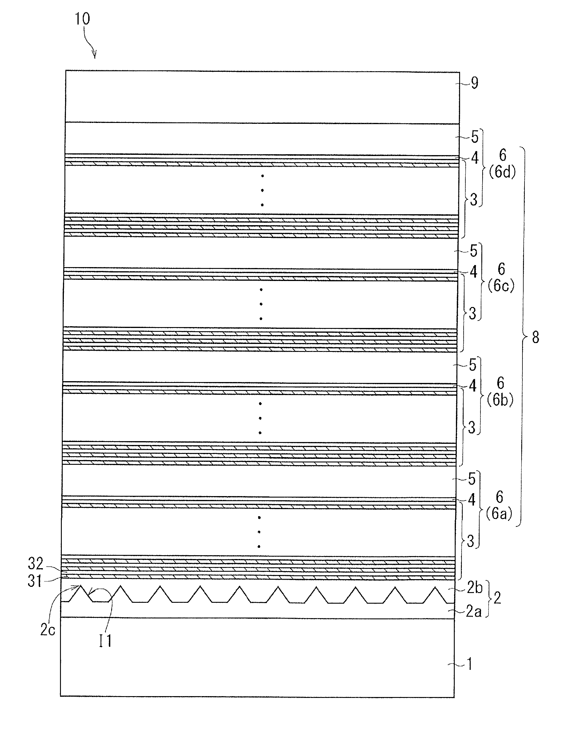
[0118]As an example, a plurality of types of epitaxial substrates 10 were prepared, which were different from one another in terms of the layer configuration of the buffer layer 8. Table 1 shows a basic configuration of the epitaxial substrates 10 according to the example, and more specifically, materials for forming the respective layers and the film thicknesses of the respective layers.

TABLE 1

[0119]As shown in Table 1, in this example, each of the base substrate 1, the base layer 2 (the first base layer 2a and the second base layer 2b), and the function layer 9 was formed of the same material and with the same film thickness for all the epitaxial substrates 10. The function layer 9 had a two-layer configuration of a channel layer and a barrier layer.

[0120]Any of the first unit layer 31 and the termination layer 4 was made of AlN. In Table 1, the film thickness of the first unit layer 31 is represented as the variable A (nm), and the film thickness of the termination layer 4 is rep...


PUM

PropertyMeasurementUnit
thicknessaaaaaaaaaa
thicknessaaaaaaaaaa
thicknessaaaaaaaaaa

Abstract

Provided is a crack-free epitaxial substrate having a small amount of warping, in which a silicon substrate is used as a base substrate. The epitaxial substrate includes: a (111) single crystal Si substrate and a buffer layer formed of a plurality of lamination units being continuously laminated. The lamination unit includes: a composition modulation layer formed of a first and a second unit layer having different compositions being alternately and repeatedly laminated such that a compressive strain exists therein; a termination layer formed on an uppermost portion of the composition modulation layer, the termination layer acting to maintain the compressive strain existing in the composition modulation layer; and a strain reinforcing layer formed on the termination layer, the strain reinforcing layer acting to enhance the compressive strain existing in the composition modulation layer.

Description

TECHNICAL FIELD[0001]The present invention relates to an epitaxial substrate for use in a semiconductor device, and particularly to an epitaxial substrate made of a group-III nitride.BACKGROUND ART[0002]A nitride semiconductor is attracting attention as a semiconductor material for a light-emitting device such as a LED or a LD and for a high-frequency / high-power electronic device such as a HEMT, because the nitride semiconductor has a wide band gap of direct transition type and the breakdown electric field and the saturation electron velocity thereof are high. For example, a HEMT (high electron mobility transistor) device in which a barrier layer made of AlGaN and a channel layer made of GaN are laminated takes advantage of the feature that causes a high-concentration two-dimensional electron gas (2DEG) to occur in a lamination interface (hetero interface) due to the large polarization effect (a spontaneous polarization effect and a piezo polarization effect) specific to a nitride m...

Claims


Application Information

Patent Timeline
Patent Type & Authority Applications(United States)
IPC IPC(8): H01L29/20H01L21/02
CPCH01L21/02381H01L21/02433H01L21/02458H01L21/02507H01L21/0262H01L29/1029H01L29/155H01L29/7787H01L29/2003H01L21/0254
Inventor MIYOSHI, MAKOTOSUMIYA, SHIGEAKIICHIMURA, MIKIYAMAEHARA, SOTATANAKA, MITSUHIRO
Owner NGK INSULATORS LTD
Why Eureka
Try Eureka