Semiconductor Wavelength Converting Devices and Light Sources for Generating Infrared Rays

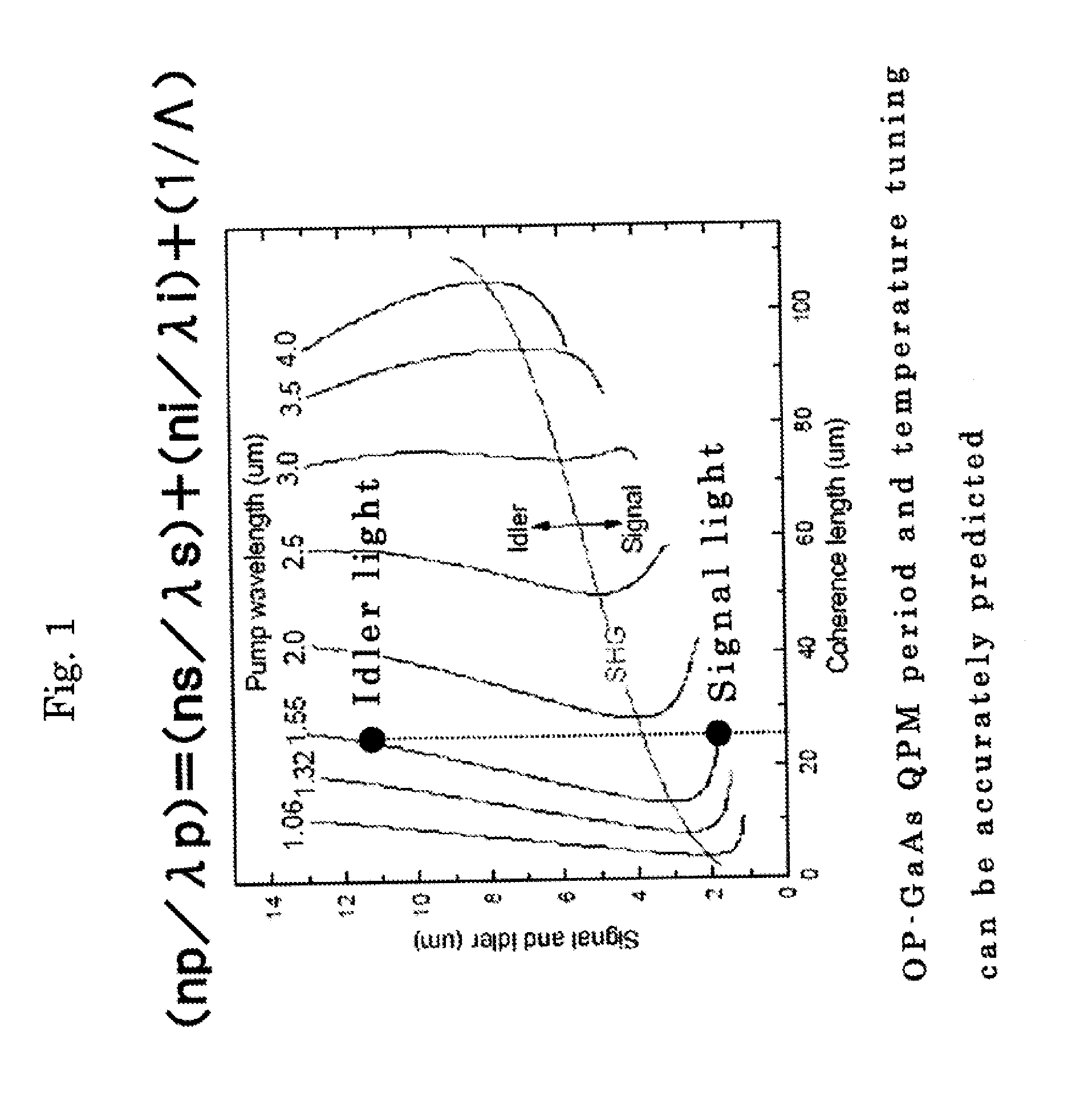
a technology of infrared rays and conversion devices, which is applied in the direction of optics, lasers, instruments, etc., can solve the problems of difficult to provide an optical waveguide of a low loss, observed roughness in the core portion, and increased propagation loss, so as to reduce the temperature distribution, and reduce the propagation loss of light.

Inactive Publication Date: 2013-06-20
NGK INSULATORS LTD
View PDF0 Cites 6 Cited by
  • Summary
  • Abstract
  • Description
  • Claims
  • Application Information

AI Technical Summary

Benefits of technology

[0031]For solving the problem described above, it was tried to make the thickness of a substrate of a non-linear optical semiconductor crystal to 50 μm or smaller to reduce the temperature distribution in the direction of the thickness. That is, a semiconductor thin plate having a thickness of 50 μm or smaller is mounted on a Peltier device used for the temperature control, and the pump light is input into the thin plate. It was, however, found that a spot size of the idler light in the direction of thickness becomes comparable with the thickness of the substrate itself, so that the light is absorbed in a metal plate forming the Peltier device and the propagation loss of the light becomes larger.
[0032]Thus, in such wavelength converting device utilizing a non-linear optical semiconductor crystal in which a Peltier device is used to control the temperature to oscillate the idler light in wavelength tunable manner, the inventors have tried to make the thickness of the wavelength converting layer to 50 μm or smaller and to provide a layer functioning as a clad between the Peltier device and wavelength converting device to prevent the absorption of light into the Peltier device. As a result, it is found that the reduction of the propagation loss of light and the increase of the spectrum line width can be prevented. The present invention is thus successfully made.

Problems solved by technology

However, after the ridge type optical waveguide including QPM is produced by semiconductor process, it is observed roughness in its core portion.
The propagation loss is thereby inevitably increased.
As described above, although the OP-GaAs has considerable potential as the wavelength converting device generating mid-and far infrared rays, it is difficult to provide an optical waveguide of a low loss.
It is, however, found that the line width of spectrum is widened to result in a reduction of output power.

Method used


Image

  • Semiconductor Wavelength Converting Devices and Light Sources for Generating Infrared Rays
  • Semiconductor Wavelength Converting Devices and Light Sources for Generating Infrared Rays
  • Semiconductor Wavelength Converting Devices and Light Sources for Generating Infrared Rays

Examples


##ventive example 1

Inventive Example 1

[0074]It was produced the wavelength converting device described referring to FIGS. 3 and 4, and it was then assembled the resonator-type infrared ray generating device described referring to FIG. 6(b).

[0075]First, main physical properties of GaAs are shown below.[0076]Density: 5.316 g / cm3 [0077]Melting point: 1238° C.[0078]Thermal Expansion coefficient: 6.86×10⁻⁶ / K at 300° C.[0079]Thermal Conduction: 55 W / m·K[0080]Dielectric constant: 11.53, 10.10 (ε0, ε∞)[0081]Refractive Index: 3.3 to 3.7

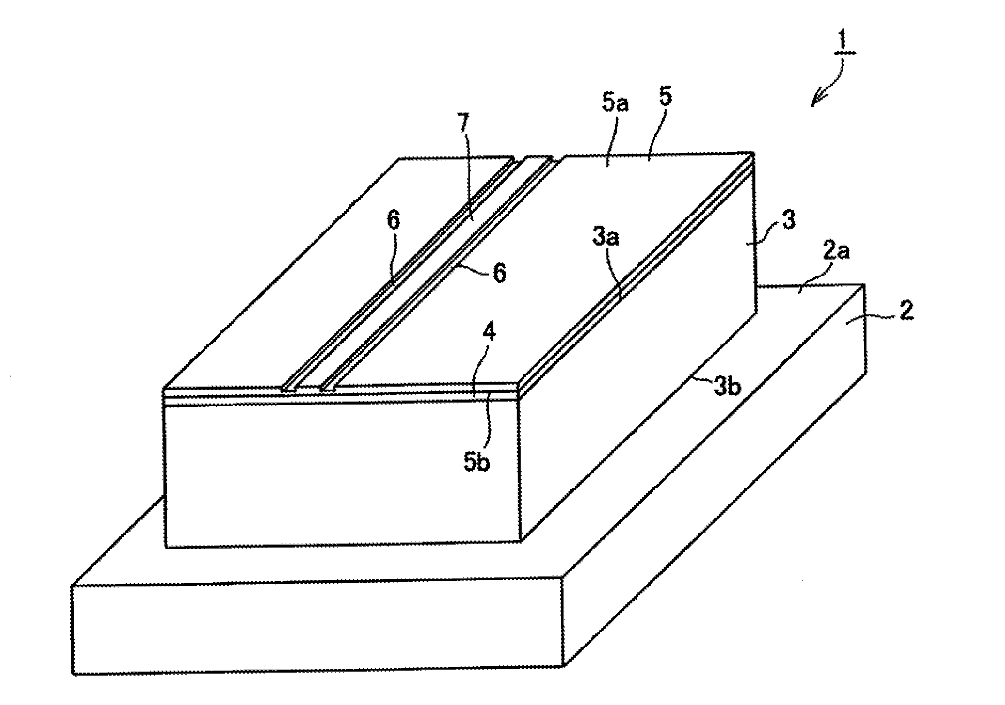
[0082]Specifically, as shown in FIG. 7, it was prepared a 2-inch OP-GaAs wafer 12 having an inversion period Λ of 58 μm. The wafer was then adhered onto a glass wafer 2 having a thermal expansion coefficient of 7 ppm / ° C. and a thickness of 0.5 mm through an adhesive layer 4 having a refractive index of 1.9 (made of Cardo polymer). The thickness of the adhesive layer was made 0.5 μg. Next, the thus adhered OP-GaAs wafer was then adhered onto a surface plate and the GaAs wafer s...

##ventive example 2

Inventive Example 2

[0087]The device 1 shown in FIGS. 3 and 4 was produced according to the same procedure as the Inventive Example 1.

[0088]Then, as shown in FIG. 6(a), the single path type infrared ray generating system was assembled.

[0089]Specifically, the OP-GaAs device with the end faces polished was mounted on the Peltier device as shown in FIG. 6(a) and a DFB laser 20 was operated at a wavelength of 1874 nm, 3 nsec and 10 μJ. Near-infrared rays (pump light) having a spectrum line width of 1 GHz was condensed with a lens and then input into the GaAs device. The orientation of the polarization of the pump light was in a crystal axis of (110). It was thus generated the idler light of a wavelength of 7333 nm whose orientation of polarization was in a crystal axis of (001). The output power was 200 nJ and spectrum line width was 2 GHz.

[0090]Further, the temperature of the Peltier device was elevated to 150° C. and it was thus proved that the wavelength of the idler light was gradual...

##ventive examples 3 and 4

Comparative Example 2 and Inventive Examples 3 and 4

[0094]FIG. 9 shows a system of generating infrared rays disclosed in the Non-Patent Reference 3 by Stanford University. Pump light P1 of a wavelength of 1.3 μm and signal light P3 of a wavelength of 1.55 μm were made incident into the wavelength converting device having the GaAs bulk same as the Comparative Example 1. The thus generated idler light was then passed through a Ge filter and outputted. The wavelength λi of the idler light was about 8 μm and output power was 114 nW.

[0095]On the other hand, the GaAs bulk device of the comparative Example 2 was replaced with the device 1 used in the above described Inventive Example 1. The output power P2 and conversion rate η of the thus obtained idler light were shown in table 2, in which “L” indicates the length of the device.

TABLE 2P1P3Lη(W)(W)(cm)(% / Wcm2)P2Comparative0.0033128.6 × 10−4114nWExample 2Inventive0.050.0520.770μWExample 3WaveguideInventive0.10.14Type1mWExample 4

[0096]As de...


PUM

PropertyMeasurementUnit
wavelengthaaaaaaaaaa
thicknessaaaaaaaaaa
wavelengthsaaaaaaaaaa

Abstract

It is provided a wavelength converting device oscillating an idler light having a wavelength of 5 to 10 μm from a pump light. The wavelength of the idler light is longer than that of the pump light. The wavelength converting device includes a wavelength converting layer 5 of a semiconductor non-linear optical crystal and having a thickness of 50 μm or smaller. The wavelength converting layer 5 includes a crystal orientation inversion structure wherein crystal orientation of the optical crystal is inverted at a predetermined period and at least one flat main face 5b. The device further includes a Peltier device 2 controlling a temperature of the wavelength converting layer 5; and a clad portion 4 joined with the flat main face 5b of the wavelength converting layer 5 and provided between the wavelength converting layer 5 and the Peltier device 2. The pump light, idler light and signal light satisfies a particular phase matching condition.

Description

[0001]This application claims the benefit of Japanese Patent Application No. P2011-276962 filed on Dec. 19, 2011, the entirety of which is incorporated by reference.TECHNICAL FIELD[0002]The present invention relates to semiconductor wavelength conversion devices and light sources for generating infrared rays.BACKGROUND ARTS[0003]Mid- and far-infrared rays in a band of wavelengths of 5 to 10 μm shows strong absorption peaks corresponding to those of various gases and living cells, so that such rays draw attention in applications of measurement and analysis based on infrared ray spectroscopy. It is, however, necessary to scan in a range of wavelengths near absorption peaks of gases or the like for performing infrared ray spectroscopy. It is thus required a light source for 5 GHz or lower whose line width of spectrum is narrow and wavelength is tunable.[0004]Although semiconductor lasers have been widely applied for gas analysis in near-infrared spectroscopy, they can be applied in a r...

Claims


Application Information

Patent Timeline
Patent Type & Authority Applications(United States)
IPC IPC(8): G02F1/35H01S3/094
CPCG02F1/35H01S3/094H01S3/2391H01S3/0092B82Y20/00G02F1/39G02F2001/3546G02F2001/3548G02F1/3556G02F1/3546G02F1/3548
Inventor KONDO, JUNGOIWATA, YUICHIEJIRI, TETSUYA
Owner NGK INSULATORS LTD
Why Eureka
Try Eureka