Eureka AIR delivers breakthrough ideas for toughest innovation challenges, trusted by R&D personnel around the world.

Electro-deposited copper-alloy foil and electro-deposited copper-alloy foil provided with carrier foil

a technology of copper alloy and carrier foil, which is applied in the direction of cell components, transportation and packaging, and other domestic articles, can solve the problems of difficult infrared laser work on copper foil, uneven composition of alloy layer in thickness direction, and extremely low absorption efficiency of copper foil in wavelength region of infrared laser, etc., to enhance infrared laser absorption efficiency, and excellent infrared laser drilling workability

Inactive Publication Date: 2013-07-04
MITSUI MINING & SMELTING CO LTD
View PDF10 Cites 5 Cited by
  • Summary
  • Abstract
  • Description
  • Claims
  • Application Information

AI Technical Summary

Benefits of technology

The present invention relates to an electro-deposited copper-alloy foil that is excellent in infrared laser-drilling workability and can be etched at a uniform speed along its thickness direction. The foil contains copper-tin alloy with tin at a specific content, which does not require a post-treatment for enhancing infrared laser absorptivity efficiency such as a black-oxide treatment. The surface-treated electro-deposited copper-alloy foil is also excellent in laser-drilling workability and includes a rust-proofing treatment, a roughening treatment for improving adhesion to a base material resin, and a silane coupling agent treatment.

Problems solved by technology

However, even when the formation of the micro via-hole in the printed wiring board should be performed by direct irradiating of a laser beam on copper foil, absorptivity of copper foil in wavelength region of an infrared laser is extremely low and it makes infrared laser working on copper foil difficult.
However, in the method disclosed in Patent Document 1 subjecting the metal Sn layer formed on the surface of copper foil to the diffusion treatment to alloy Sn and Cu (that is, form the alloy layer mainly composed of Sn and Cu), composition of the alloy layer in the thickness direction will be uneven.
The matter causes deviations in the etching rate along the thickness direction in the following etching process and it makes formation of a desired wiring pattern difficult.
Further, in the conventional methods disclosed in Patent Documents 1 and 2, it is difficult to reduce a manufacturing cost because the surface of copper foil should be subjected to the treatment for enhancing the infrared laser absorptivity, i.e. the methods include indispensable additional steps in a manufacturing process.

Method used


Image

  • Electro-deposited copper-alloy foil and electro-deposited copper-alloy foil provided with carrier foil
  • Electro-deposited copper-alloy foil and electro-deposited copper-alloy foil provided with carrier foil
  • Electro-deposited copper-alloy foil and electro-deposited copper-alloy foil provided with carrier foil

Examples


example 1

[0050]In Example 1, a surface-treated electro-deposited copper-alloy foil provided with a carrier foil was prepared by a method described below. Then a metal-clad laminate was prepared and infrared laser-drilling workability was evaluated by using the metal-clad laminate. Hereinafter, process steps in Example 1 will be described one by one.

[Preparation of Surface-Treated Electro-Deposited Copper-Alloy Foil Provided with Carrier Foil]

[0051]The surface-treated electro-deposited copper-alloy foil provided with a carrier foil prepared in Example 1 was prepared through the following steps 1 to 4. Respective steps will be described.

[0052]Step 1: In the step 1, an electro-deposited copper foil having a thickness of 18 μm was used as a carrier foil, and a releasing layer was formed on one surface having surface roughness (Rzjis) of 0.6 μm. The surface roughness was measured by a probe type surface roughness measuring meter according to JIS B 0601 using a diamond stylus of which tip radius i...

example 2

[0068]In Example 2, a surface-treated electro-deposited copper-alloy foil having a thickness of 3 μm was formed with the condition described below where composition of copper-tin plating bath and electrolysis condition in the step 3 in Example 1 were changed. Then, a peelable-type surface-treated electro-deposited copper-alloy foil provided with a carrier foil was prepared in the same manner as in Example 1.

[Composition of Copper-Tin Plating Bath and Electrolysis Condition]

[0069]CuSO4.5H2O: 79 g / l (Cu: 20 g / L)

[0070]SnSO4: 72 g / l (Sn: 40 g / L)

[0071]C6H11O7Na: 70 g / l

[0072]H2SO4: 70 g / l

[0073]Solution temperature: 45° C.

[0074]Cathode current density: 15 A / dm2

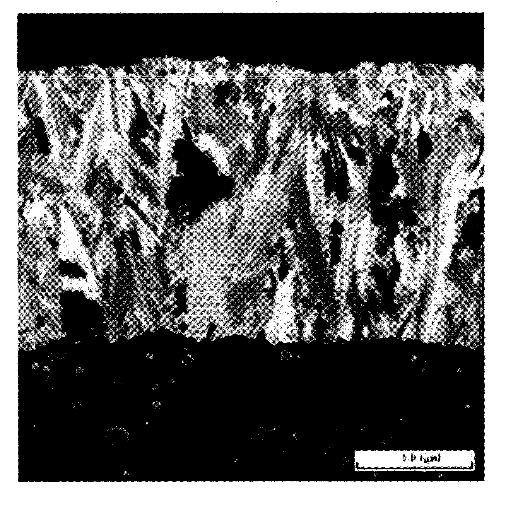
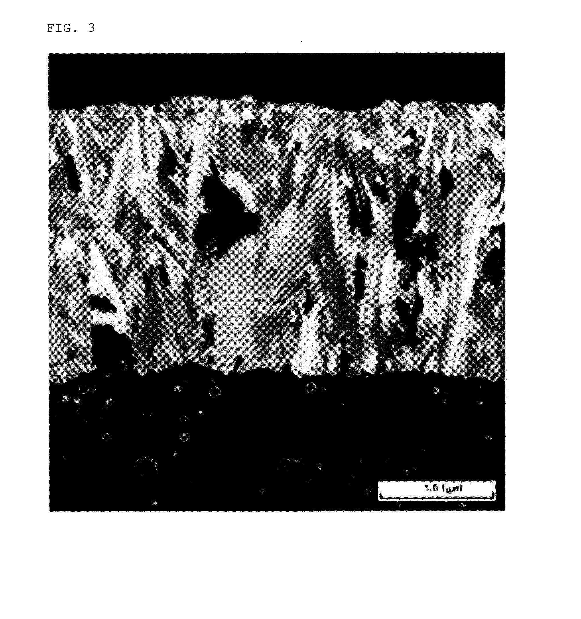
[0075]Tin content of the surface-treated electro-deposited copper-alloy foil constituting the surface-treated electro-deposited copper-alloy foil provided with the carrier foil was 12.9% by mass. FIG. 5 shows an image of a cross-sectional crystal structure of the surface-treated electro-deposited copper-alloy foil cut in parallel to ...


PUM

PropertyMeasurementUnit
thicknessaaaaaaaaaa
thicknessaaaaaaaaaa
diameteraaaaaaaaaa

Abstract

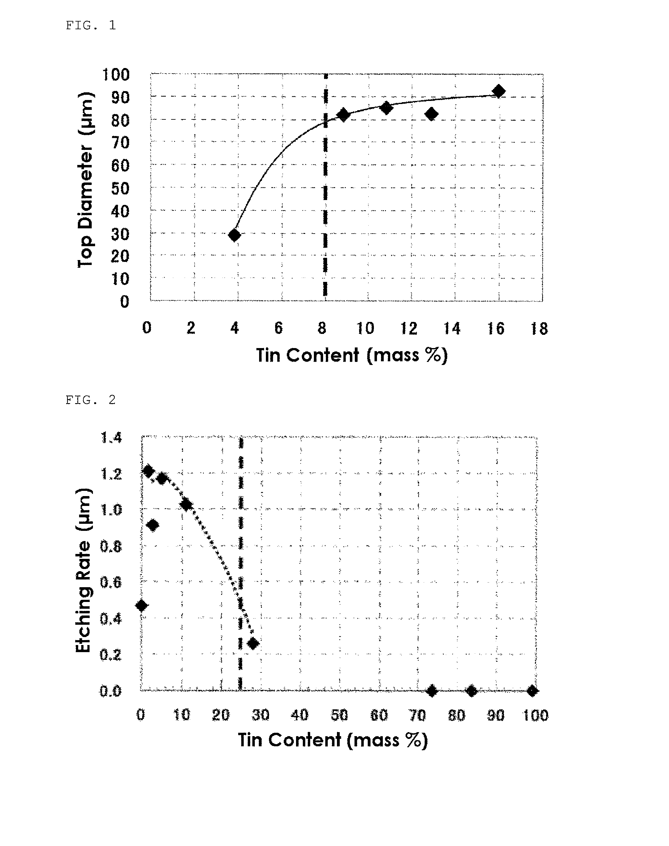
An object of the present invention is to provide an electro-deposited copper-alloy foil excellent in infrared laser processability which enables uniform etching rate along a thickness direction in following etching process. To achieve the object, an electro-deposited copper-alloy foil obtained from electrolyzing of an electrolytic solution, wherein the electro-deposited copper-alloy foil has tin content of 8% by mass to 25% by mass is employed. In the electro-deposited copper-alloy foil, a grain in a crystal structure is preferably a columnar grain longitudinal along a thickness direction.

Description

BACKGROUND OF THE INVENTION[0001]1. Field of the Invention[0002]The present invention relates to an electro-deposited copper-alloy foil. In particular, the present invention relates to an electro-deposited copper-alloy foil suitable for a printed wiring board use.[0003]2. Description of the Related Art[0004]In recent years, a device space in a printed wiring board used for supplying an electric signal tends to be narrowed depending on high performance and downsizing of electronic and electric devices. The matter requires downsized high-density mounting on the printed wiring board. Then, a micro via-hole has been provided in the printed wiring board suitable for high density mounting to electrically conduct plural layers.[0005]However, even when the formation of the micro via-hole in the printed wiring board should be performed by direct irradiating of a laser beam on copper foil, absorptivity of copper foil in wavelength region of an infrared laser is extremely low and it makes infr...

Claims


Application Information

Patent Timeline
Patent Type & Authority Applications(United States)
IPC IPC(8): C25D7/06B32B15/20
CPCB32B2260/021B32B2457/08B32B15/20C25D3/58C25D7/0614C25D1/04Y10T428/31663Y10T428/31678
Inventor MATSUDA, MITSUYOSHIYOSHIKAWA, KAZUHIROFUJIMOTO, TAKAO
Owner MITSUI MINING & SMELTING CO LTD
Why Eureka
Eureka Blog
Learn More