Variable resistive element, and non-volatile semiconductor memory device

a resistive element and non-volatile technology, applied in the direction of bulk negative resistance effect devices, semiconductor devices, electrical appliances, etc., can solve the problems of difficult control of current influence, difficult to reduce the current required for switching to be less than about 10 a, and difficult to control the influence of current, etc., to achieve high work function, easy application, and large energy gap

Inactive Publication Date: 2013-08-01
SHARP KK +1
View PDF5 Cites 24 Cited by
  • Summary
  • Abstract
  • Description
  • Claims
  • Application Information

AI Technical Summary

Benefits of technology

[0059]The process that can easily form a film in non-equilibrium state, such as a sputtering method, is used for forming a film of the metal oxide so as to form the metal oxide film that has the oxygen composition ratio satisfying the above-mentioned condition, whereby the resistance change layer and the high-oxygen layer can be formed.
[0060]The variable resistive element is formed to have an asymmetric structure in which an interface between one of the first electrode and the second electrode and the oxide becomes an ohmic junction or a state close to the ohmic junction, while an interface between the other electrode and the oxide becomes a state such as a schottky junction where energy gap of conductive carriers is caused. With this configuration, the resistance state of the variable resistive element is changed between the high resistance state and the low resistance state by the application of voltage pulses having different polarities. The filament is opened and closed on the interface between the electrode, to which an electric field is easily applied, and which has relatively large energy gap, and the oxide. Therefore, the variable resistive element according to the present invention can be realized by the structure in which the resistance change layer is in contact with the one (here, the second electrode), having relatively a high work function, of both electrodes.
[0061]As a result, the variable resistive element can easily be driven by using a microfabricated transistor having low breakdown voltage. Consequently, the variable resistive element that can perform a stable switching operation with low voltage and small current can be realized. A high-integrated large-capacity non-volatile semiconductor memory device including the variable resistive element can easily be realized.

Problems solved by technology

However, there arises a problem that writing by random access cannot be performed during the erasing action since the erasing action is performed on a block basis.
This is because it is difficult to control the influence of current spike to a parasitic capacitance during the forming.
On the other hand, in the variable resistive element using hafnium oxide or zirconium oxide, it is difficult to reduce the current required for the switching to be not more than about 10 μA to 100 μA only by the current control by the transistor.
However, in the metal oxide having very strong coupling between metal and oxygen, such as hafnium oxide and zirconium oxide, the amount of applied voltage and current necessary for forming the filament path is large.
Therefore, it is difficult to form a small filament path, which means it is difficult to reduce the switching current.
As a result, leak current (current upon dielectric breakdown) rapidly increases.
Accordingly, it is difficult to perform the forming with small current such as in nanoampere order, so that a small filament is difficult to form, which means it is difficult to perform resistance switching with low voltage and small current.

Method used


Image

  • Variable resistive element, and non-volatile semiconductor memory device
  • Variable resistive element, and non-volatile semiconductor memory device
  • Variable resistive element, and non-volatile semiconductor memory device

Examples


first embodiment

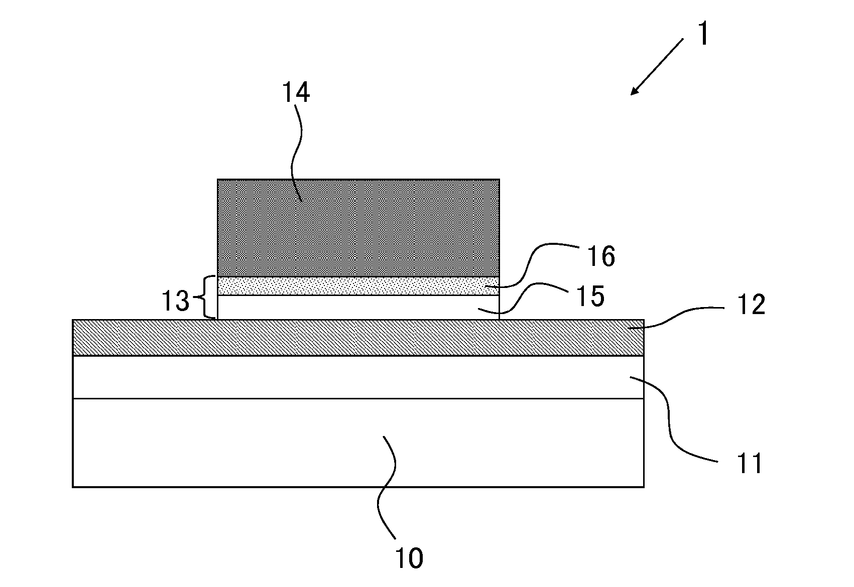
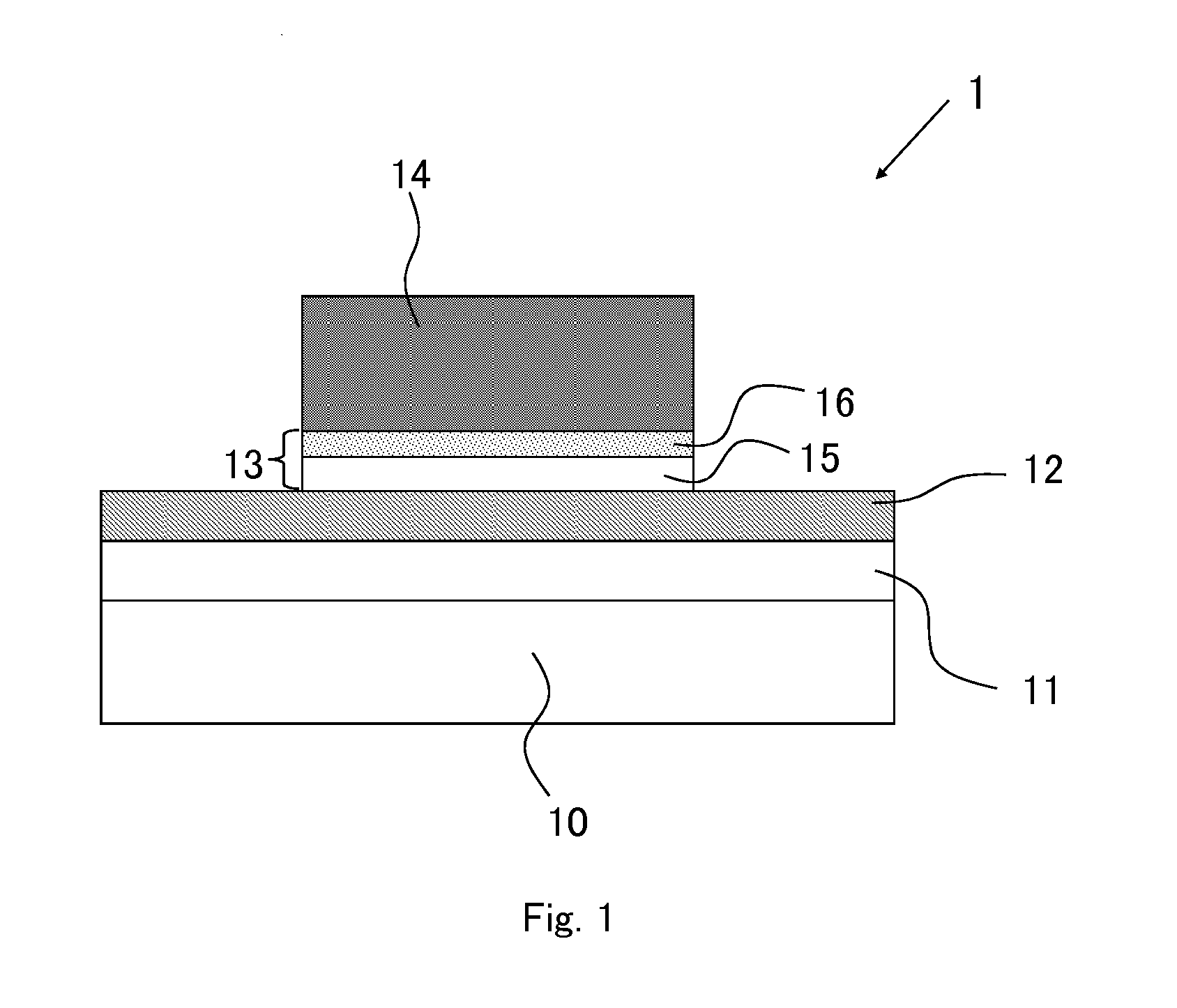
[0078]FIG. 1 is a sectional view schematically illustrating a structure of a variable resistive element 1 (hereinafter appropriately referred to as “present element 1”) according to one embodiment of the present invention.

[0079]In the drawings described below, essential parts are emphasized for the sake of convenience of description, and a dimensional ratio of each component of the element and an actual dimensional ratio do not agree with each other in some cases.

[0080]The variable resistive element 1 includes a second electrode (lower electrode) 12, a variable resistor 13, and a first electrode (upper electrode) 14, those of which are deposited and patterned in this order on an insulating film 11 formed on a substrate 10. The variable resistor 13 includes at least two layers which are a resistance change layer 15 and a high-oxygen layer 16, and each of which is made of a metal oxide film or a metal oxynitride film.

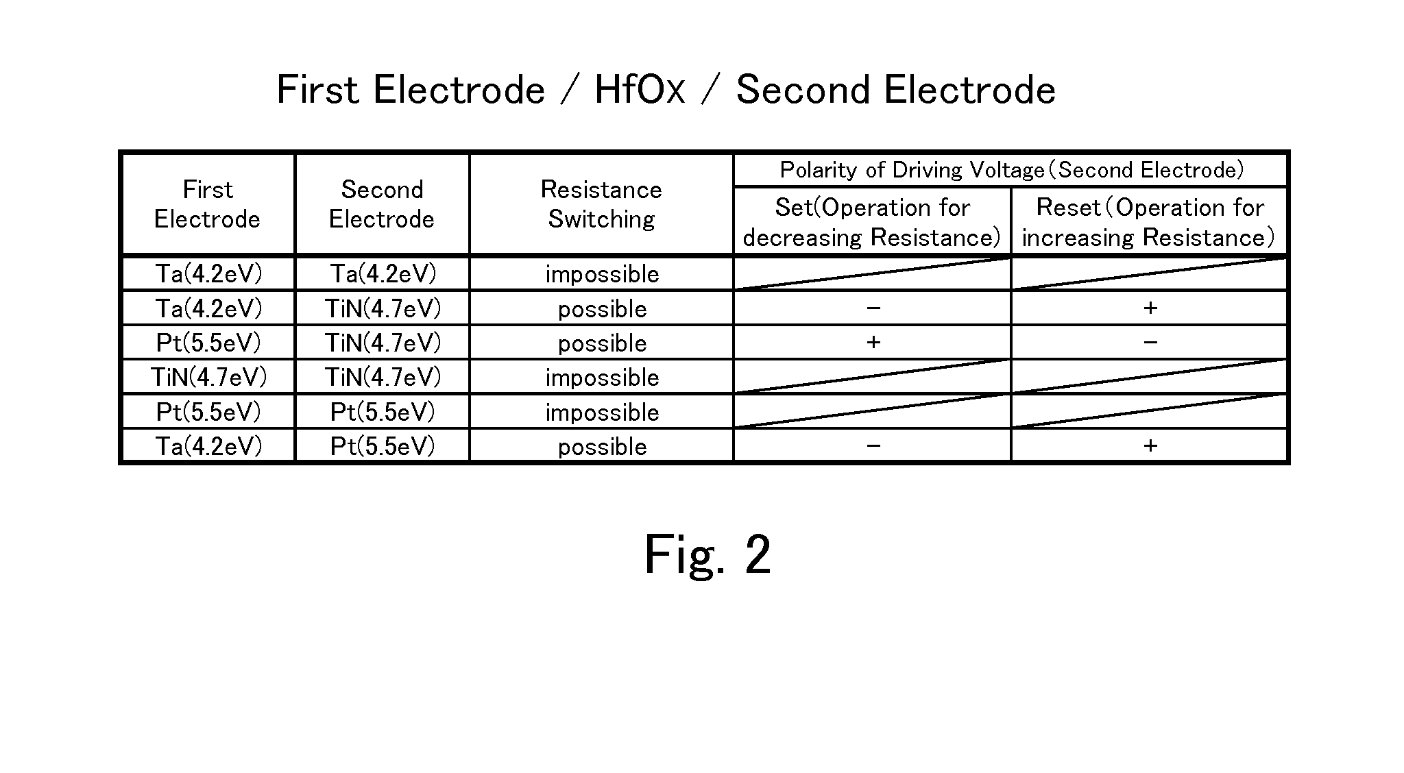
[0081]In the present embodiment, hafnium oxide (HfOX) that has a lar...

second embodiment

[0106]In the first embodiment described above, the present element 1 includes the resistance change layer 15 and the high-oxygen layer 16, these layers being made of the same metal oxide but having different oxygen defect concentration. However, the resistance change layer 15 and the high-oxygen layer 16 may be made of a different metal oxide. The resistance change of the variable resistive element appears since oxygen atoms are collected or diffused by the electric field near the interface between the electrode and the variable resistor. Therefore, it is more preferable that the high-oxygen layer 16 is made of a different oxide or oxynitride having free energy of formation of oxide higher than that of the oxide or oxynitride forming the resistance change layer 15. This structure facilitates the oxygen transfer from the high-oxygen layer 16 to the resistance change layer 15 during the reset operation, whereby the reset current, which is difficult to control only by the limitation of...

third embodiment

[0114]FIG. 8 illustrates a non-volatile semiconductor memory device using the present element 1 or 2 described above. FIG. 8 is a circuit block diagram illustrating a schematic configuration of a non-volatile semiconductor memory device 20 (hereinafter referred to as “present device 20” as needed) according to one embodiment of the present invention. As illustrated in FIG. 8, the present device 20 includes a memory cell array 21, a control circuit 22, a voltage generating circuit 23, a word-line decoder 24, a bit-line decoder 25, and a source-line decoder 26.

[0115]The memory cell array 21 includes a plurality of memory cells, each of which includes the variable resistive element R, in at least one of a row direction and a column direction in a matrix. The memory cells belonging to the same column are connected by a bit line extending in the column direction, and the memory cells belonging to the same row are connected by a word line extending in the row direction. The memory cell ar...


PUM


Abstract

A variable resistive element that performs a forming action at small current and a stable switching operation at low voltage and small current, and a low-power consumption large-capacity non-volatile semiconductor memory device including the element are realized. The element includes a variable resistor between first and second electrodes. The variable resistor includes at least two layers, which are a resistance change layer and high-oxygen layer, made of metal oxide or metal oxynitride. The high-oxygen layer is inserted between the first electrode having a work function smaller than the second electrode and the resistance change layer. The oxygen concentration of the metal oxide of the high-oxygen layer is adjusted such that the ratio of the oxygen composition ratio to the metal element to stoichiometric composition becomes larger than the ratio of the oxygen composition ratio to the metal element of the metal oxide forming the resistance change layer to stoichiometric composition.

Description

CROSS REFERENCE TO RELATED APPLICATION[0001]This Nonprovisional application claims priority under 35 U.S.C. §119(a) on Patent Application No. 2012-017024 filed in Japan on Jan. 30, 2012 the entire contents of which are hereby incorporated by reference.BACKGROUND OF THE INVENTION[0002]1. Field of the Invention[0003]The present invention relates to a variable resistive element storing information based upon an electric operating characteristic in which a resistance changes due to application of electric stress, and to a non-volatile semiconductor memory device using the variable resistive element.[0004]2. Description of the Related Art[0005]A non-volatile memory represented by a flash memory has widely been used for a computer, communication, measuring device, automatic control device, and device for daily use in a personal life, as a high-capacity and compact information recording medium. A demand for an inexpensive and high-capacity non-volatile memory has been extremely increased. ...

Claims


Application Information

Patent Timeline
Patent Type & Authority Applications(United States)
IPC IPC(8): H01L45/00
CPCH01L45/145H01L45/08H01L45/1233H01L27/249H01L45/146H01L45/1625H01L27/2436H01L45/1253H10B63/30H10B63/845H10N70/24H10N70/826H10N70/841H10N70/8833H10N70/883H10N70/026
Inventor NAKANO, TAKASHITAMAI, YUKIOASANO, ISAMUAIZAWA, KAZUO
Owner SHARP KK
Why Eureka
Try Eureka