Devices Including Metal-Silicon Contacts Using Indium Arsenide Films and Apparatus and Methods

Active Publication Date: 2013-08-08
APPLIED MATERIALS INC
View PDF1 Cites 235 Cited by
  • Summary
  • Abstract
  • Description
  • Claims
  • Application Information

AI Technical Summary

Benefits of technology

[0008]One aspect of the present invention pertains to a substrate processing apparatus. In embodiments of this aspect, the apparatus comprises a first processing chamber to clean a substrate to provide a cleaned substrate; a second processing chamber in communication with the first processing chamber to deposit a layer comprising indium arsenide on the cl

Problems solved by technology

However, insertion of a high bandgap oxide with a large conduction band offset result

Method used


Image

  • Devices Including Metal-Silicon Contacts Using Indium Arsenide Films and Apparatus and Methods
  • Devices Including Metal-Silicon Contacts Using Indium Arsenide Films and Apparatus and Methods
  • Devices Including Metal-Silicon Contacts Using Indium Arsenide Films and Apparatus and Methods

Examples


Embodiment Construction

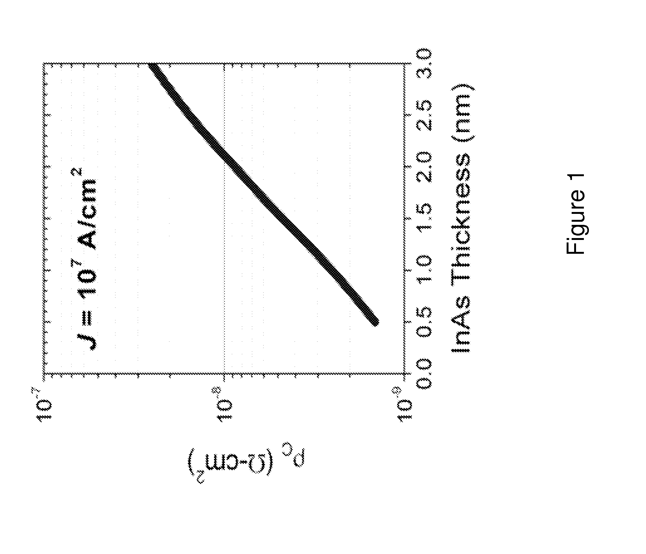
[0025]It has been found that using indium arsenide (InAs) films as an interfacial layer in transistor contacts provides contact resistivities below 1×10⁻⁸ ohm-cm2. Thus, various embodiments described herein provide methods and apparatuses for the forming thin InAs layers on a substrate surface.

[0026]As used herein, a “substrate surface,” refers to any substrate or material surface formed on a substrate upon which film processing is performed during a fabrication process. For example, a substrate surface on which processing can be performed include materials such as silicon, silicon oxide, strained silicon, silicon germanium, silicon carbide, silicon on insulator (SOI), carbon doped silicon oxides, silicon nitride, doped silicon, germanium, gallium arsenide, indium arsenide, indium gallium arsenide, indium aluminum arsenide, glass, sapphire, and any other materials such as metals, metal nitrides, metal alloys, and other conductive materials, depending on the application. Barrier laye...


PUM

PropertyMeasurementUnit
Temperatureaaaaaaaaaa
Thicknessaaaaaaaaaa

Abstract

Described are apparatus and methods for forming films comprise indium and arsenic. In particular, these films may be formed in a configuration of two or more chambers under “load lock” conditions. These films may include additional components as dopants, such as aluminum and/or gallium. Such films can be used in metal/silicon contacts having low contact resistances. Also disclosed are devices including the films comprising indium arsenide.

Description

CROSS-REFERENCE TO RELATED APPLICATIONS[0001]This application claims the benefit under 35 U.S.C. §119(e) to U.S. Provisional Application No. 61 / 591,066, filed Jan. 26, 2012, and U.S. Provisional Application No. 61 / 595,371, filed Feb. 6, 2012, the entire contents of which are incorporated herein by reference in their entirety.FIELD[0002]Embodiments of the present invention generally relate to the field of semiconductor manufacturing processes and devices, particularly to apparatus and methods for forming devices such as field effect transistors including indium arsenide films providing low contact resistivity.BACKGROUND[0003]Microelectronic devices are fabricated on a semiconductor substrate as integrated circuits in which various conductive layers are interconnected with one another to permit electronic signals to propagate within the device. An example of such a device is a complementary metal-oxide-semiconductor (CMOS) field effect transistor (FET) or MOSFET.[0004]An exemplary FET...

Claims


Application Information

Patent Timeline
IPC IPC(8): H01L21/768H01L23/482H01L21/67
CPCH01L21/76843H01L21/6715H01L23/4827H01L21/6719H01L29/772H01L21/28525H01L2924/0002H01L21/67207H01L2924/00C23C14/22C23C16/0227C23C16/45544C23C16/52
Inventor AHMED, KHALED Z.GOPALRAJA, PRABUNOORI, ATIFCHANG, MEI
Owner APPLIED MATERIALS INC
Why Eureka
Try Eureka