

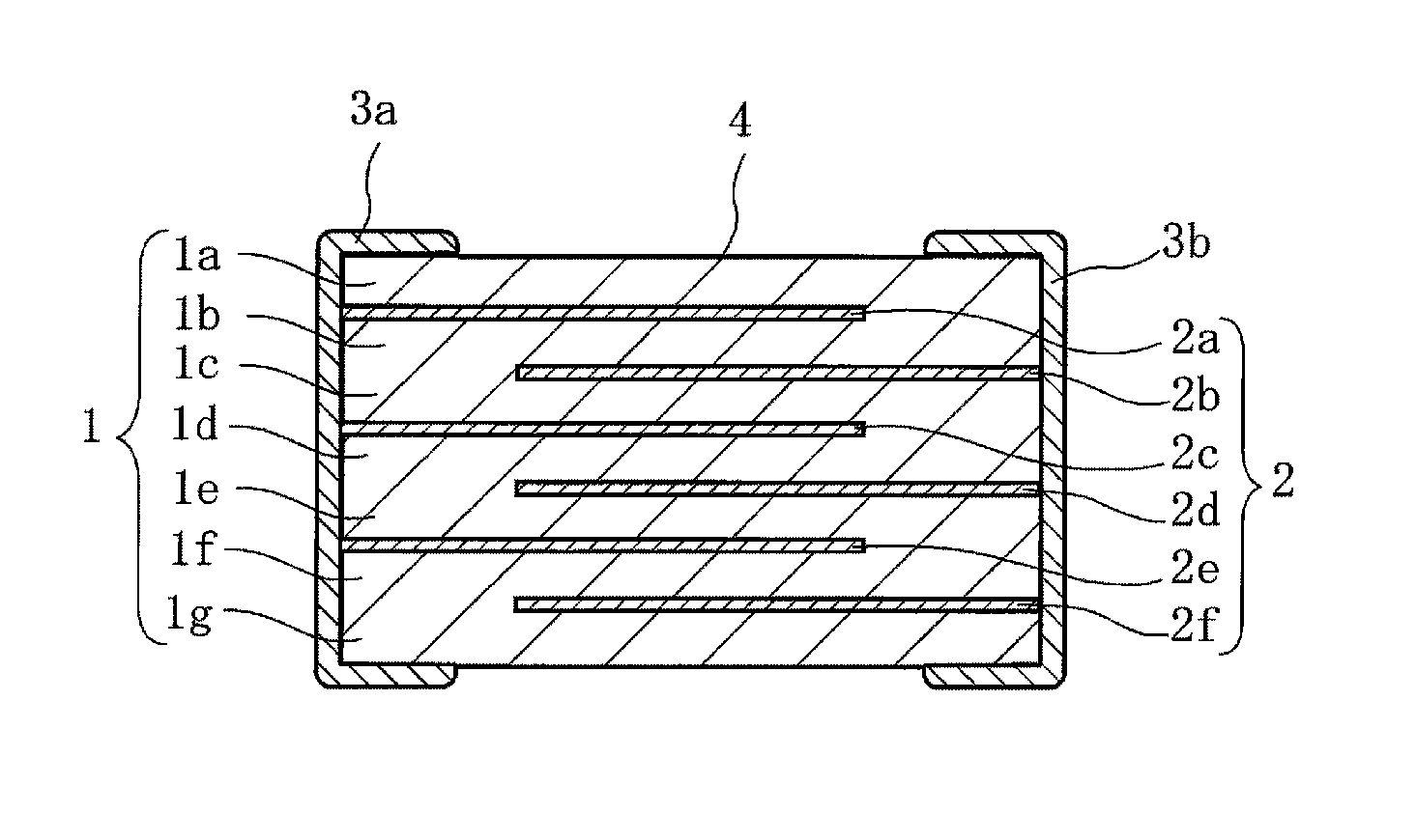
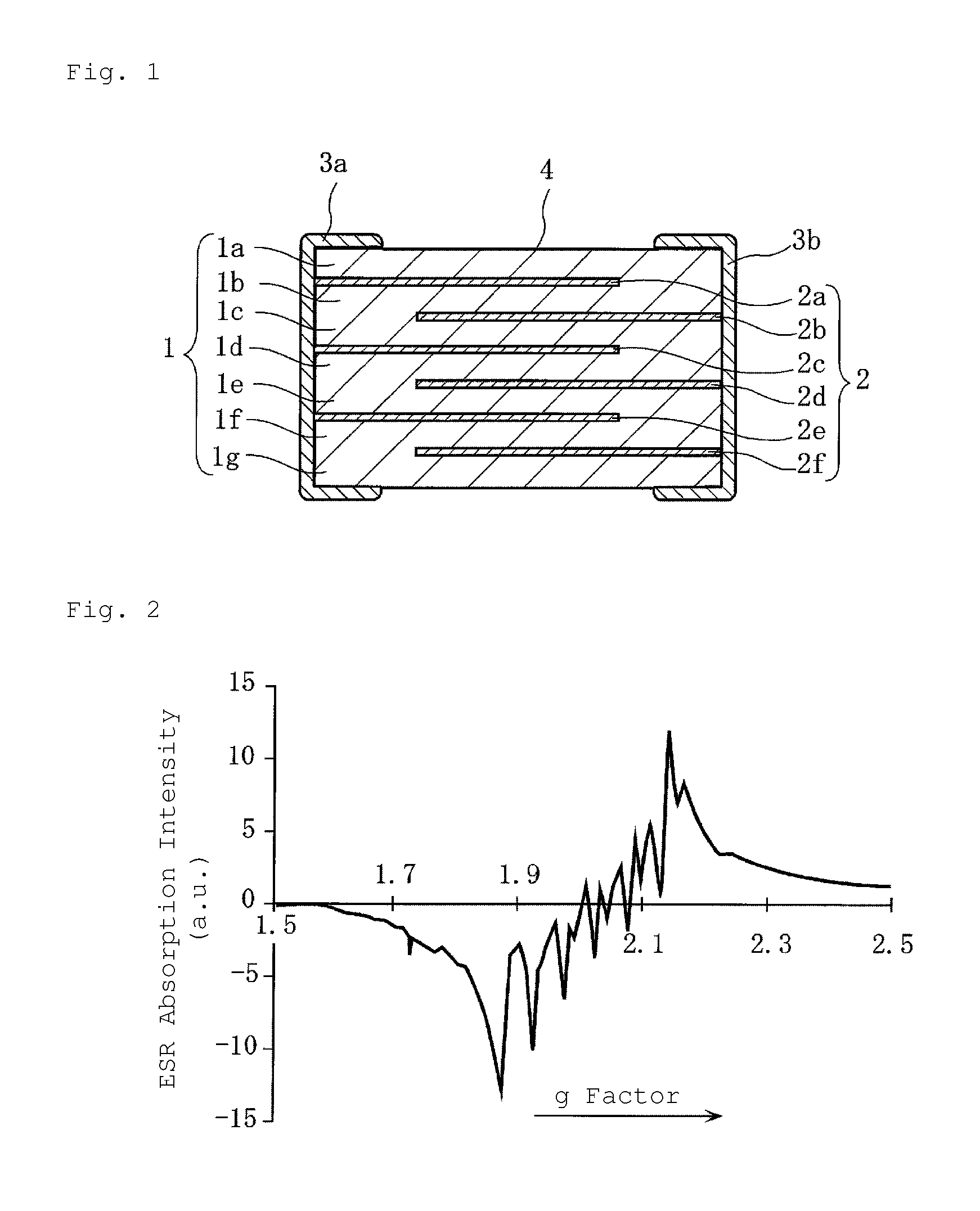
Semiconductor ceramic and method for manufacturing the same, and laminated semiconductor ceramic capacitor with varistor function and method for manufacturing the same
a semiconductor ceramic and varistor technology, applied in the direction of fixed capacitors, non-conductive materials with dispersed conductive materials, solid-state devices, etc., can solve the problems of capacitor itself being broken, semiconductor elements to be broken, capacitors themselves not functioning to absorb high-voltage pulses or static electricity, etc., to suppress varistor characteristics, high efficiency, and stable characteristics
- Summary
- Abstract
- Description
- Claims
- Application Information
AI Technical Summary
Benefits of technology
Problems solved by technology
Method used
Image

Examples
examples
Preparation of Sample
Sample No. 1
[0111]As ceramic raw materials, SrCO3, TiO2 having a specific surface area of 30 m2 / g (average grain diameter: about 30 nm), and LaCl3 as a donor compound were prepared. Then, LaCl3 was weighed in such a way that the content of La was 0.8 mol with respect to 100 mol of the Ti element, and further SrO3 and TiO2 were weighed in such a way that the compounding molar ratio m of a Sr site to a Ti site (=Sr site / Ti site) was 1.000.
[0112]Three parts by weight of ammonium polycarboxylate were added to 100 parts by weight of these weighed materials as a dispersant, and then the resulting mixture was charged into a ball mill with PSZ balls of 2 mm in diameter as a pulverizing medium and pure water, and subjected to wet mixing for 16 hours in the ball mill to prepare a slurry.
[0113]Next, this slurry was evaporated to dryness, and then subjected to a calcination treatment at a temperature of 1400° C. for 2 hours in the atmosphere of the air to obtain a calcined ...
PUM
| Property | Measurement | Unit |
|---|---|---|
| Temperature | aaaaa | aaaaa |
| Temperature | aaaaa | aaaaa |
| Length | aaaaa | aaaaa |
Abstract
Description
Claims
Application Information