
Electro-Depositing Metal Layers of Uniform Thickness

a technology of uniform thickness and metal layer, applied in the field of thin film photovoltaic cells and semiconductor wafer electrodeposition, can solve the problems of poor thickness and composition uniformity, non-uniform thickness deposited on the cathodic substrate, etc., and achieve the elimination or substantially minimization of electrolyte agitation, uniform plating thickness, and elimination of convective flow

Inactive Publication Date: 2013-09-26
TECHNIC INC
View PDF0 Cites 8 Cited by
  • Summary
  • Abstract
  • Description
  • Claims
  • Application Information

AI Technical Summary

Benefits of technology

The patent describes a method for electroplating metals onto a substrate with uniform thickness distribution. Two main modifications are needed: eliminating or minimizing external agitation of the electrolyte and choosing an appropriate effective current density. These modifications have resulted in improved thickness distribution when compared to traditional electroplating methods. Horizontal disposing of the electrodes further reduces convective flows and mixing of the electrolyte. The technique can be applied to manufacturing PV cells and other semiconductor devices. The patent also discusses a previous study that used electro-deposition without external agitation, but the results showed non-uniform thickness distribution.

Problems solved by technology

Other than the studies disclosed herein, the only other basic scientific study in which electroplating without agitation, in an unstirred bath, was used resulted in layers of non-uniform thickness deposited on the cathodic substrate.
The authors reported significant variations in composition over the surface of the cathode and concluded that plating from unstirred electrolyte leads to poor thickness and composition uniformity.

Method used


Image

  • Electro-Depositing Metal Layers of Uniform Thickness
  • Electro-Depositing Metal Layers of Uniform Thickness
  • Electro-Depositing Metal Layers of Uniform Thickness

Examples


example 1

Copper, Without External Agitation

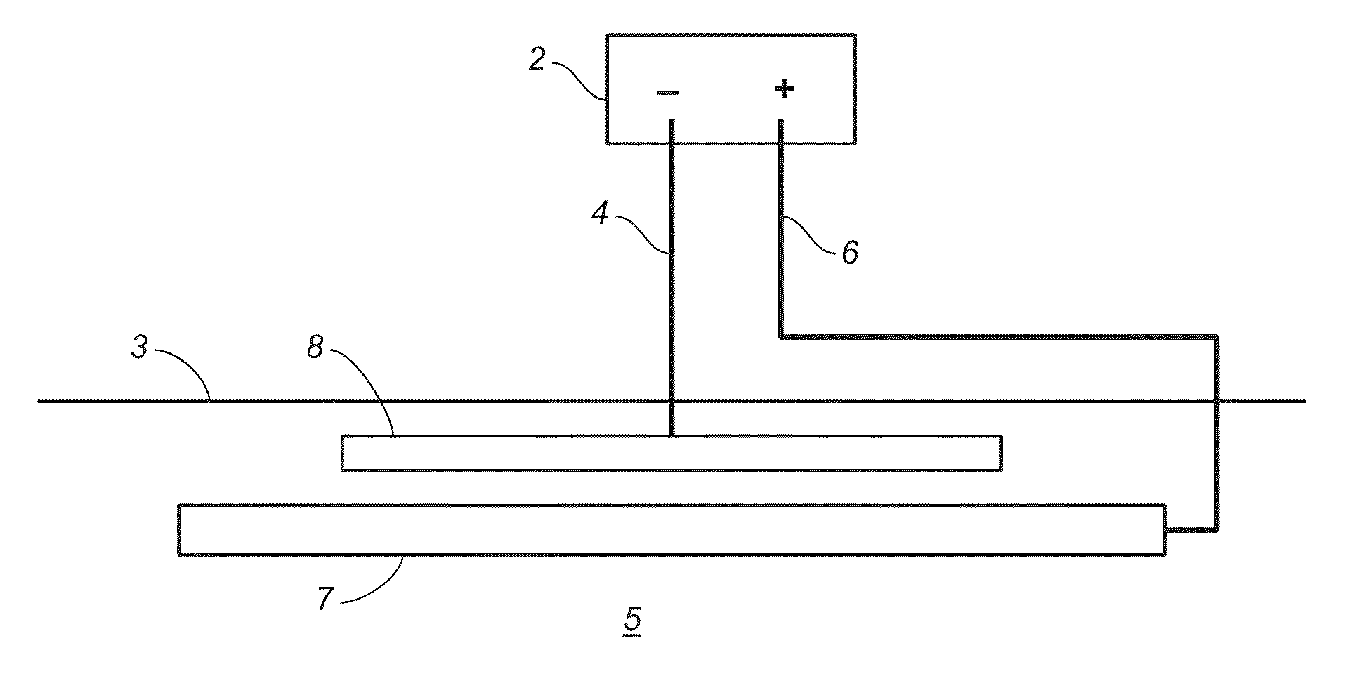
[0039]A cathode substrate composed of polyimide film sputtered with Mo and a 100 nm Cu seed layer having the dimensions of 23 cm by 14 cm was immersed in an 11% solution of sulfuric acid, containing 7.5 grams per liter (gm / l) copper as copper sulfate and 5 ml / l D-2 brightener (Technic Inc.), 6 ml / l D-120 Carrier (Technic Inc.) and 70 ppm chloride ions, for 3.5 minutes at 1.5 A (4.3 ASF), at a plating temperature of 20°. The cathode was positioned horizontally and parallel to a copper foil anode with a spacing of 0.4 cm between the anode and the cathode. The plating process was carried out without any external agitation during the plating process.

[0040]The results are graphically illustrated in FIG. 6, with the vertical axis indicating the thickness of the copper plated onto the cathodic substrate in nanometers and the horizontal axis indicating positions along the substrate's plated surface. The mean thickness of the substrate after electroplating w...

example 2

Copper, With External Agitation

[0041]The process according to Example 1 was carried out, except that the plating process was carried out with liquid agitation of the plating solution via reciprocating horizontal movement of the cathode substrate.

[0042]The results are graphically illustrated in FIG. 7, with the vertical axis indicating the thickness of the copper plated onto the cathodic substrate in nanometers and the horizontal axis indicating positions along the substrate's plated surface. The mean thickness of the copper plated on the substrate after electroplating was 220 nm, with a standard deviation of 170, coefficient of variation 77.3%. The effect of external agitation on the thickness uniformity of the deposition as compared to Example 1 can readily be seen. Deposits of up to about 500 nm thick formed at the edges of the substrate whereas deposits of only about 100-200 nm thick formed elsewhere.

example 3

Copper, Without External Agitation, Insufficient Current Density

[0043]The process according to Example 1 was carried out except that the copper concentration was increased to 30 gm / l (instead of 7.5) and the plating process was run for 10 minutes (instead of 3.5). No increase in cell potential was observed during the plating interval.

[0044]The results are graphically illustrated in FIG. 8, with the vertical axis indicating the thickness in nanometers of the copper plated onto the cathodic substrate and the horizontal axis indicating positions along the substrate's plated surface. The mean thickness of the copper plated on the substrate after electroplating was 584 nm, the standard deviation was 607, and the coefficient of variation was 104%. At the increased copper concentration, the current density was insufficient to form an ion-depleted layer with a concentration over-potential that increases during the plating process. Consequently, the Cu deposits at the edges of the substrate ...


PUM

PropertyMeasurementUnit
Thicknessaaaaaaaaaa
Electric potential / voltageaaaaaaaaaa
Current densityaaaaaaaaaa

Abstract

The invention is an apparatus and method for forming highly uniform layers of metal on a substrate by electro-deposition. The substrate is electroplated in a bath composed of a quiescent (i.e., no external agitation) electrolyte solution using an effective constant current density carefully selected to match the chemical composition of the electrolyte.

Description

FIELD OF THE INVENTION[0001]The invention is in the field of electroplating in general, and more particularly to thin film photovoltaic cell and semi-conductor wafer electro-deposition, as well as in other applications in which uniform layers of the plated metal or metal alloy are required.BACKGROUND OF THE INVENTION[0002]The current initiative to implement solar photovoltaic power generation on a large scale has created interest in low cost methods of photovoltaic cell (PV cell) fabrication. Traditionally, PV cells have been made from crystalline silicon wafers with a thickness ranging from 150-350 microns. Silicon-based PV cells are expensive because of the amount of raw material required and the necessity of removing impurities and defects from the silicon. In addition, silicon has a band gap energy of 1.1 eV, which is at the lower end of the range of effectiveness for PV cells. Thin-film semi-conducting alloys, which are fabricated from two or more semiconductor layers having di...

Claims


Application Information

Patent Timeline
IPC IPC(8): C25D21/12B32B15/04
CPCC25D3/56C25D17/12C25D7/123Y10T428/12681B32B15/043C25D21/12Y10T428/12826C25D5/003
Inventor HRADIL, GEORGE
Owner TECHNIC INC
Learn More