Multi-Layered Phase-Change Memory Device

a memory device and phase-change technology, applied in the field of memory devices, can solve problems such as the challenge of the reliability of the pcm

Active Publication Date: 2013-11-07
FENG CHIA UNIVERSITY
View PDF13 Cites 18 Cited by
  • Summary
  • Abstract
  • Description
  • Claims
  • Application Information

AI Technical Summary

Benefits of technology

[0016]It can be learnt from prior arts that new materials of Phase-Change Memory (PCM) is not usable as its crystallization temperature is rather low benchmarking to that of GST (160˜180° C.). If thickness of the film in PCM is too thin, such as in the case of 2 nm or 1.5 nm, reliability of the PCM is challenged due to difficulty in process control of homogeneity within 0.1 nm thickness in large area. Accordingly, the present invention proposes a way that a film made of pure Antimony (Sb) or Bismuth (Bi) is sandwiched between an upper and a lower barrier layers forming a single sandwich-memory-unit to solve the above problems. The crystallization temperature of the Sb film in a sandwich-memory-unit can be raised obviously due to both the sandwiching and the thickness effect. This means that Tc of the Sb (or Bi) film inside can be adjusted by barrier materials used for the sandwiching. On the other hand Tc of thinner Sb (or Bi) film inside the sandwich-memory-unit is also higher.

Problems solved by technology

If thickness of the film in PCM is too thin, such as in the case of 2 nm or 1.5 nm, reliability of the PCM is challenged due to difficulty in process control of homogeneity within 0.1 nm thickness in large area.

Method used


Image

  • Multi-Layered Phase-Change Memory Device
  • Multi-Layered Phase-Change Memory Device
  • Multi-Layered Phase-Change Memory Device

Examples


embodiment 1

[0127]The undoped Sb-film as the phase-change material is made into a bridge-memory-device which means that the operation current is applied to flow parallel to the plane of the Sb-film. The processing of this device is as follow: at the deposition rate of 0.33 nm / min, a Sb-film is deposited on SiO2 / Si with the thickness of 5 nm. It is inevitably contaminated with trace impurity of oxygen. The Sb-film is deposited between the first electrode 300 which is the left electrode in FIG. 10, and the second electrode which is the right electrode in the FIG. 10. A layer of silicon oxide with the thickness of 100 nm is deposited on top of the Sb-film which is then sandwiched between two barrier SiO2 layers. Focused ion beam (FIB) is used to cut the sandwiched Sb-film into bridge memory device with a length of 1000 nm and a width of 200 nm. The sectional view is observed by the transmission electron microscopy (TEM) shown as the inset in FIG. 10.

[0128]FIG. 10 also illustrates relationship betw...

embodiment 2

[0130]In this preferable embodiment, a three-layered sandwich structure made of undoped Sb film is made into a vertical memory device, which means that operation current flows vertical to the plane of the Sb-film. First, bottom electrode TiN, which acts also as the conductive barrier layer, is deposited onto SiO2 / Si substrate. After deposition of a dielectric layer SiO2, two vias with sizes of 400 nm, and 800 square nanometers, respectively, are prepared by photolithography by the back-end-of-line of a complementary-metal-oxide-semiconductor (CMOS) processing. Undoped Sb-film is deposited into the vias at the deposition rate of 0.33 nm / min until the thickness of 5 nm. Thereafter, the TaN top electrode, which also acts as another conductive barrier layer, is deposited. FIG. 11 illustrates electrical resistance (Ω)-voltage (V) during set and reset operations of the vertical memory-cell made of undoped Sb-film with 400 square nanometers. The pulse width is 100 ns. The set voltage is 2....

embodiment 3

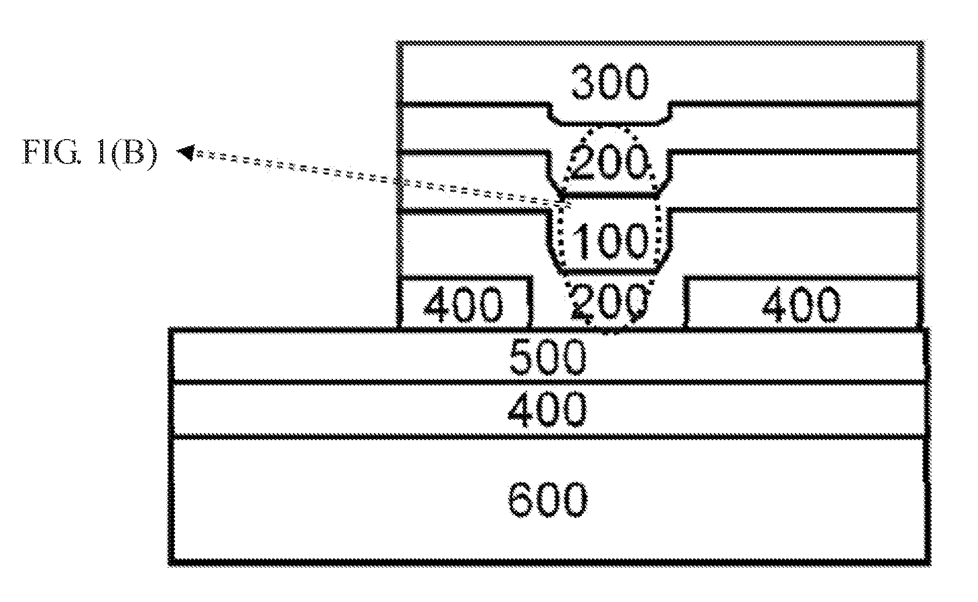
[0132]In this preferable embodiment, 8 at % carbon doped single Sb-phase film (C8at%), at 10 nm thickness, is made into a vertical memory-cell and tested by the processes described in Embodiment 2. With Sb(C) as the memory material, the memory-layer 100 is can be connected with the electrodes on upper and lower sides. Cell structure is a three-layered sandwich-structure the same as that shown in the FIG. 1 (A). The material of the electrodes and the barrier layer is nitrides, TiN on the bottom and TaN on top. Silicon oxide formed by a low temperature process is adopted as the material of the dielectric layer 400. The deposition rate of the memory-layer 100 is 0.33 nm / min.

[0133]FIG. 13 illustrates the electrical resistance (Ω)—applied voltage (V) curve (R-V curve) of the memory cell upon set-reset is carried out using a pulse-width of 80 ns. With I-sweep mode, electrical resistance of the vertical memory cell at originally high resistance state can be switched to the low resistance s...


PUM


Abstract

The invention discloses a phase-change memory device structure and the materials used. The structure includes a substrate; a single or multiple sandwich-memory-unit(s); a first and a second electrode electrically connecting to the first and the second sides of the sandwich-memory-units and a dielectric layer used as the insulator required by the memory device. The sandwich-memory-unit composes of a memory-layer, thinner than 30 nm, sandwiched between an upper and a lower barrier-layers. The barrier-layer is either an electrical conductor in case of vertical memory-cells or an electrical insulator in case of parallel memory-cells. The sandwich-memory-unit is characteristic of increased crystallization temperature of at least 50° C. as the thickness of the memory-layer is reduced from 15 to 5 nm; and the volume change of the memory-layer is less than 3% during phase change. The thickness and memory-material in each sandwich-memory-unit can be different in the multiple sandwich-memory-units.

Description

BACKGROUND OF THE INVENTION[0001]1. Field of the Invention[0002]The present invention is related to a memory device, more particularly to structures and materials of a non-volatile phase-change memory device.[0003]2. Description of Prior Art[0004]Along with technology advancement, demands for a high quality non-volatile memory have been asked for. Except for high reliability, fast operation speed, high cyclability and large storage capacity become basic requirements. Accordingly, various types of non-volatile memories (NVM) for the next generation are emerging. These include but not limited to Magnetoresistive Random Access Memory (MRAM), Oxide-based Resistive Random Access Memory (RRAM), Ferroelectric Random Access Memory (FRAM), and Phase-Change Memory (PCM). Among them PCM utilizes a material whose phases can be changed rapidly and reversibly between an amorphous phase and a counterpart crystalline phase. Moreover, high electrical resistance of the amorphous phase and low electri...

Claims


Application Information

Patent Timeline
Patent Type & Authority Applications(United States)
IPC IPC(8): H01L45/00
CPCH01L45/1253H10N70/823H10N70/841H10N70/231H10N70/884H10N70/023H10N70/826B82Y10/00
Inventor CHIN, TSUNG-SHUNECHANG, CHIH-CHUNGCHU, YUNG-CHING
Owner FENG CHIA UNIVERSITY
Why Eureka
Try Eureka