Eureka AIR delivers breakthrough ideas for toughest innovation challenges, trusted by R&D personnel around the world.

Photomask blank and method for manufacturing photomask

Active Publication Date: 2013-11-21
SHIN ETSU CHEM IND CO LTD
View PDF4 Cites 8 Cited by
  • Summary
  • Abstract
  • Description
  • Claims
  • Application Information

AI Technical Summary

Benefits of technology

The present invention relates to a structure that includes a hard mask film made of a chromium-containing material including tin on an inorganic material film. This film can cause an increase in etching rate during chlorine-containing dry etching and also shows resistance to fluorine-containing dry etching, reducing the burden on the photoresist and enabling high-precision pattern transfer even with a thinned resist film.

Problems solved by technology

However, there is a possibility of causing insufficient etching resistance of a hard mask film when etching a film under the hard mask film by only sufficiently reducing the thickness of the hard mask film to secure high precision of patterning.
In addition, it is very difficult to improve etching resistance while maintaining high resolution from the side of a photoresist material.
However, there is a problem that such a chromium-containing material of rich in light element and low in chromium composition should have a large film thickness for the purpose of a decrease in etching resistance to fluorine-containing dry etching and assure a sufficient function as a hard mask film.

Method used


Image

  • Photomask blank and method for manufacturing photomask
  • Photomask blank and method for manufacturing photomask
  • Photomask blank and method for manufacturing photomask

Examples


example 1

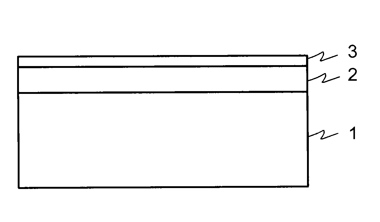
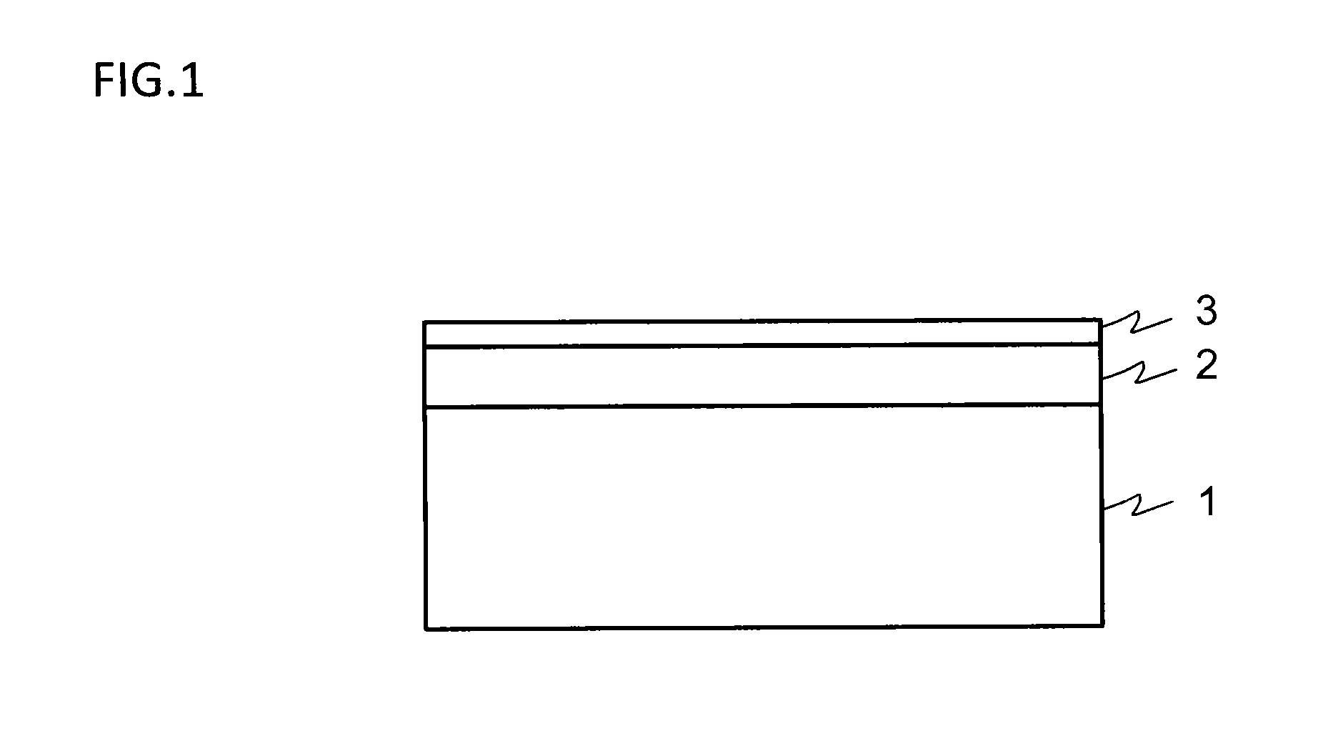
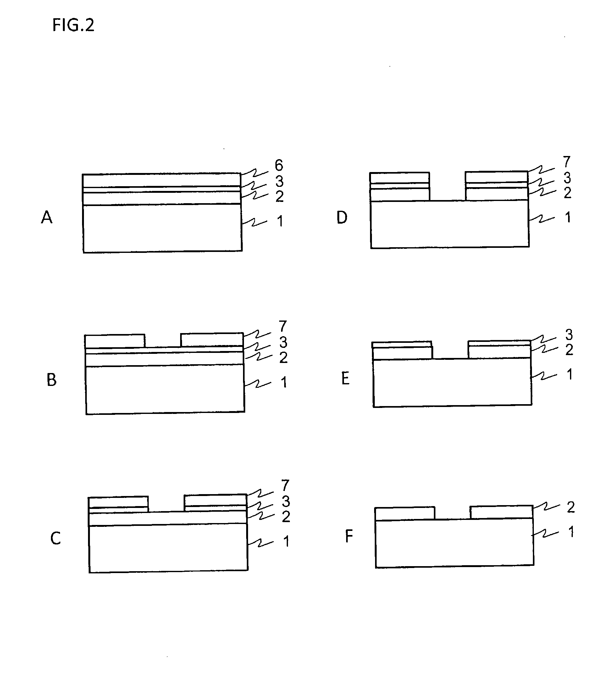
[0127]A light-shielding film including a light-shielding layer and an anti-reflection layer was formed on a quartz substrate by using a direct-current sputtering device. As a light-shielding layer, a film (41 nm in film thickness) made of molybdenum, silicon, and nitrogen was formed on the quartz substrate.

[0128]Using two different targets, a MoSi2 target and a Si target, as targets, film-formation was performed on the quartz substrate in rotation at 30 rpm. Sputtering gas used was Ar and nitrogen and adjusted so that the inside of a gas chamber could have a gas pressure of 0.05 Pa.

[0129]When the composition of this light-shielding film was investigated by ESCA, it was Mo:Si:N=3:1:5 (atomic ratio).

[0130]On the light-shielding layer, film-formation of an anti-reflection layer (10 nm in film thickness) made of molybdenum and silicon was performed by using a direct-current sputtering device.

[0131]Using two different targets, a MoSi2 target and a Si target, as targets, film-formation wa...

example 2

[0142]A half-tone phase shift film (75 nm in film thickness) made of molybdenum, silicon, oxygen, and nitrogen was formed on a quartz substrate by using a direct-current sputtering device.

[0143]Using two different targets, a MoSi2 target and a Si target, as targets, film-formation was performed on the quartz substrate in rotation at 30 rpm. Sputtering gas used was Ar and oxygen and adjusted so that the inside of a gas chamber could have a gas pressure of 0.05 Pa.

[0144]When the composition of this half-tone phase shift film was investigated by ESCA, it was Mo:Si:O:N=1:4:1:4 (atomic ratio).

[0145]Using a direct sputtering device, an etching stopper film (10 nm in film thickness) made of CrSnON was formed on the half-tone phase shift film.

[0146]Using two different targets, a Cr target and a Sn target, as targets, film-formation was performed on the quartz substrate in rotation at 30 rpm. Sputtering gas used was Ar, nitrogen, and oxygen and adjusted so that the inside of a gas chamber co...


PUM


Abstract

A light-shielding film 2 is formed on a transparent substrate 1. A hard mask film 3 is formed on this light-shielding film 2. The entire hard mask film 3 is made of a chromium-containing material including tin. The film made a chromium-containing material including tin can cause a significant increase in the etching rate at the time of chlorine-containing dry etching. Furthermore, comparing with a film made of a chromium-containing material in which part of chromium is replaced with a light element, the above film has an equal or higher level of etching resistance to fluorine-dry etching. Thus, burden on a photoresist at the time of etching the chromium-containing material film can be reduced. Therefore, high-precision pattern transfer can be performed even in the case that the resist film is thinned.

Description

TECHNICAL FIELD [0001]The present invention relates to a photomask blank for a photomask used in manufacture of a semiconductor integrated circuit or the like. More specifically, the present invention relates to a photomask blank having a hard mask film as a mask-pattern processing auxiliary film, and a method for manufacturing a photomask using such a mask blank.BACKGROUND ART [0002]In the field of semiconductor technology, research and development for further refinement of patterns have been progressed. In recent years, particularly, with high integration of a large scale integration circuit, refinement of circuit patterns, wiring patterns, or contact-hole patterns for wiring between layers forming a cell has been progressed, and a request for microfabrication technology has been increased.[0003]In connection with this, even in the field of technology for photomask production to be used in the process for photolithography in microfabrication, a technique for forming fine and corre...

Claims


Application Information

Patent Timeline
IPC IPC(8): G03F1/50G03F1/80
CPCG03F1/50G03F1/80G03F1/32G03F1/54G03F1/20G03F1/38H01L21/0273G03F1/26
Inventor FUKAYA, SOUICHINAKAGAWA, HIDEOSASAMOTO, KOUHEI
Owner SHIN ETSU CHEM IND CO LTD
Why Eureka
Eureka Blog
Learn More