Organic electroluminescent device

Active Publication Date: 2013-12-12
HODOGAYA KAGAKU IND
View PDF2 Cites 11 Cited by
  • Summary
  • Abstract
  • Description
  • Claims
  • Application Information

AI Technical Summary

Benefits of technology

[0042]The organic EL device of the present invention has a distinguished feature in that the hole-transporting layer is formed by using the arylamine compound (X) that has three or more triphenylamine skeletons in a molecule thereof and the arylamine compound (Y) that has two triphenylamine skeletons in a molecule thereof.
[0043]Namely, the hole-transporting layer that contains the arylamine compounds (X) an

Problems solved by technology

Therefore, use of the above hole-transporting material is accompanied by a problem in that the holes partly pass through the luminous layer to deteriorate the efficiency.
With the materials that are used, however, none of the luminous efficiency, driving voltage or device life is still satisfactory.
Therefore, the conventional organic EL devices are affected by the surface roughness of the transparent electrode such as ITO electrode which is used as the anode and a probability of producing defective products

Method used


Image

  • Organic electroluminescent device
  • Organic electroluminescent device
  • Organic electroluminescent device

Examples


example 1

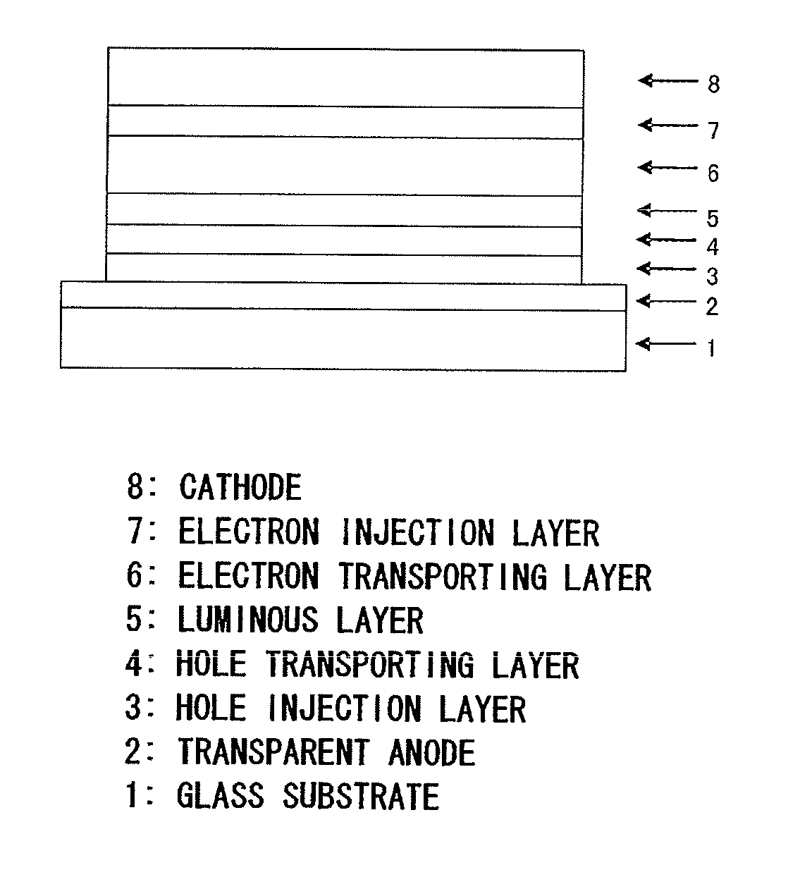
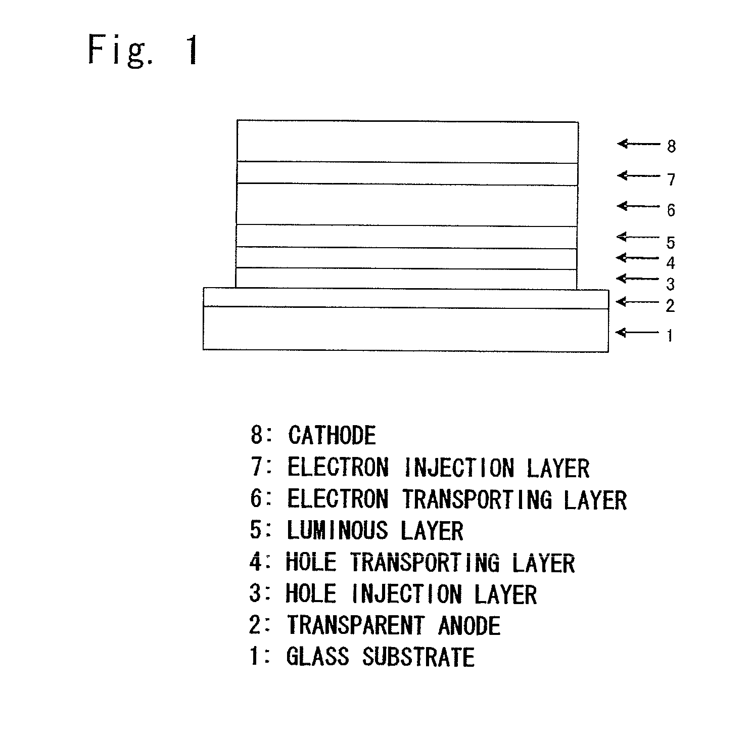
[0108]An organic EL device of a structure shown in FIG. 1 was fabricated according to the procedure described below. Namely, the organic EL device has a structure in which a transparent anode 2 (ITO electrode), a hole injection layer 3, a hole-transporting layer 4, a luminous layer 5, an electron-transporting layer 6, an electron injection layer 7 and a cathode (aluminum electrode) 8 are formed by vacuum evaporation in this order on a glass substrate 1.

[0109]First, the glass substrate 1 on which the ITO (indium tin oxide) film has been formed in a thickness of 150 nm was washed with ultrasonic waves in an isopropyl alcohol for 20 minutes and was, thereafter, dried on a hot plate heated at 200° C. for 10 minutes followed by a treatment with UV ozone for 5 minutes. Thereafter, the glass substrate with ITO was placed in a vacuum evaporation machine, and the pressure therein was decreased down to 0.001 Pa or lower.

[0110]Next, the hole injection layer 3 was formed in a thickness of 20 nm...

example 2

[0117]An organic EL device was fabricated under the same conditions as in Example 1 but forming the hole-transporting layer 4 in a thickness of 40 nm by the two-way vacuum evaporation by using the above compound (1-1) and the compound (2-1) at such deposition rates that the weight ratio thereof was 10:90.

[0118]The thus fabricated organic EL device was measured for its properties in the atmosphere at normal temperature. Table 1 summarizes the measured results of luminous properties of when a DC voltage was applied to the organic EL device.

example 3

[0119]An organic EL device was fabricated under the same conditions as in Example 1 but forming the hole-transporting layer 4 in a thickness of 40 nm by the two-way vacuum evaporation by using the above compound (1-1) and the compound (2-1) at such deposition rates that the weight ratio thereof was 40:60.

[0120]The thus fabricated organic EL device was measured for its properties in the atmosphere at normal temperature. Table 1 summarizes the measured results of luminous properties of when a DC voltage was applied to the organic EL device.


PUM


Abstract

An organic electroluminescent device comprising, between an anode and a cathode, a hole-transporting layer, a luminous layer and an electron-transporting layer, wherein the hole-transporting layer contains an arylamine compound (X) having a molecular structure to which three or more triphenylamine skeletons are singly bonded or bonded through a divalent hydrocarbon group and an arylamine compound (Y) having a molecular structure to which two triphenylamine skeletons are singly bonded or bonded through the divalent hydrocarbon group. The device excels in hole and electron injection/transport property, stability and durability in the form of thin films, and is highly efficient, becomes luminous on a low driving voltage, and has a long life.

Description

TECHNICAL FIELD[0001]This invention relates to an organic electroluminescent device which is a spontaneously luminescent device suited for use in various kinds of display devices. More specifically, the invention relates to an organic electroluminescent device (hereinafter often abbreviated as organic EL device) using specific arylamine derivatives.BACKGROUND ART[0002]An organic EL device is a spontaneously luminous device which features higher brightness and higher legibility than those of the liquid crystal devices enabling vivid display to be attained and has, therefore, been vigorously studied.[0003]In 1987, C. W. Tang et al. of the Eastman Kodak Co. have developed a device of a layer-laminated structure comprising various kinds of materials to bear individual roles, and have put an organic EL device using organic materials into a practical use. The above device is constituted by laminating layers of a phosphorescent body capable of transporting electrons and an organic material...

Claims


Application Information

Patent Timeline
IPC IPC(8): H01L51/00
CPCH01L51/0059H01L51/0072C09K11/06C09K2211/1007C09K2211/1011C09K2211/1014C09K2211/1029H05B33/14C07C211/54C07C211/56C07C211/58H05B33/10C07C2601/14C07C2603/18H10K85/631H10K2102/103H10K85/6572
Inventor YOKOYAMA, NORIMASAHAYASHI, SHUICHITAKAHASHI, EIJIKUSANO, SHIGERU
Owner HODOGAYA KAGAKU IND
Why Eureka
Try Eureka