

Semiconductor device
- Summary
- Abstract
- Description
- Claims
- Application Information
AI Technical Summary
Benefits of technology
Problems solved by technology
Method used
Image

Examples
embodiment 1
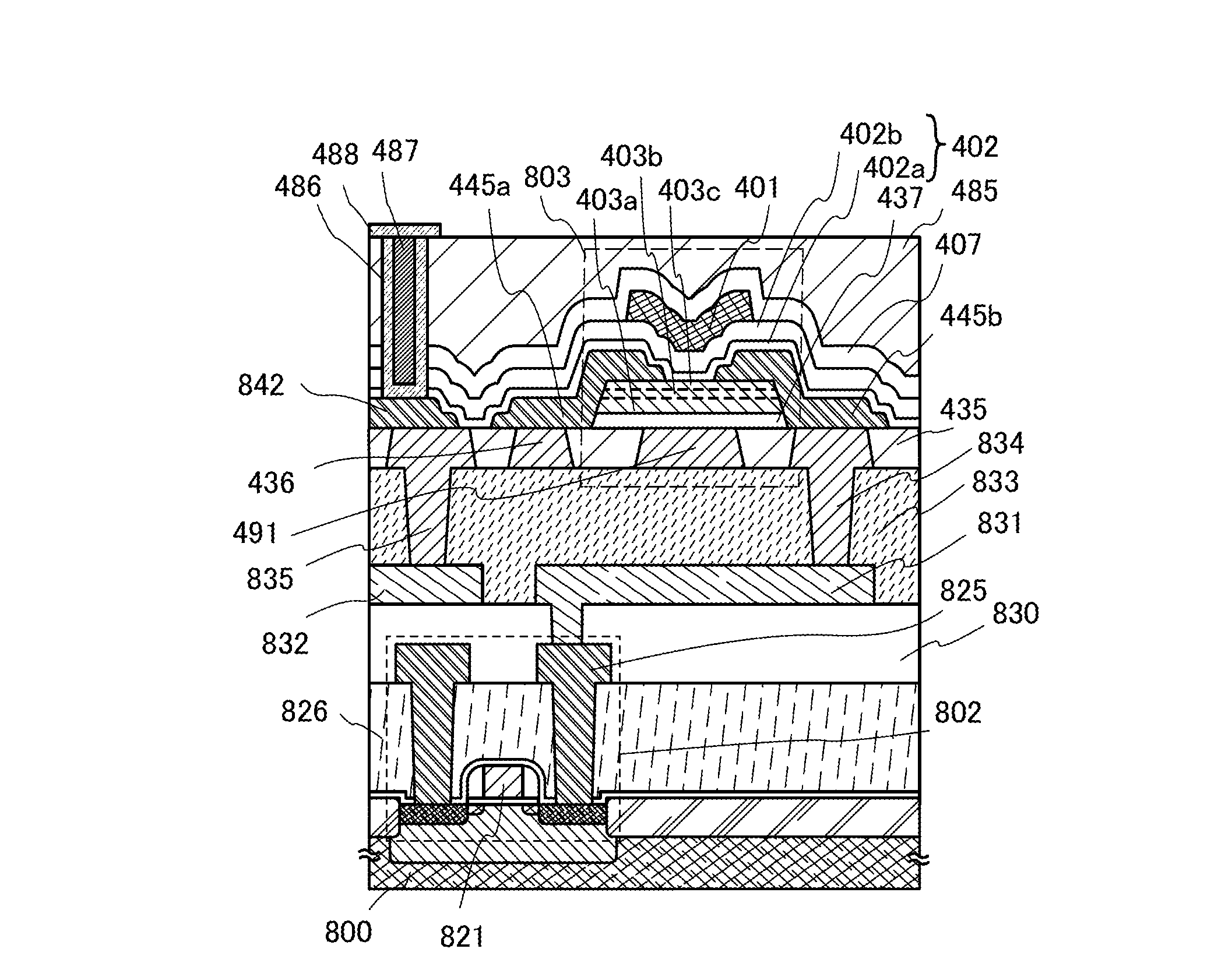
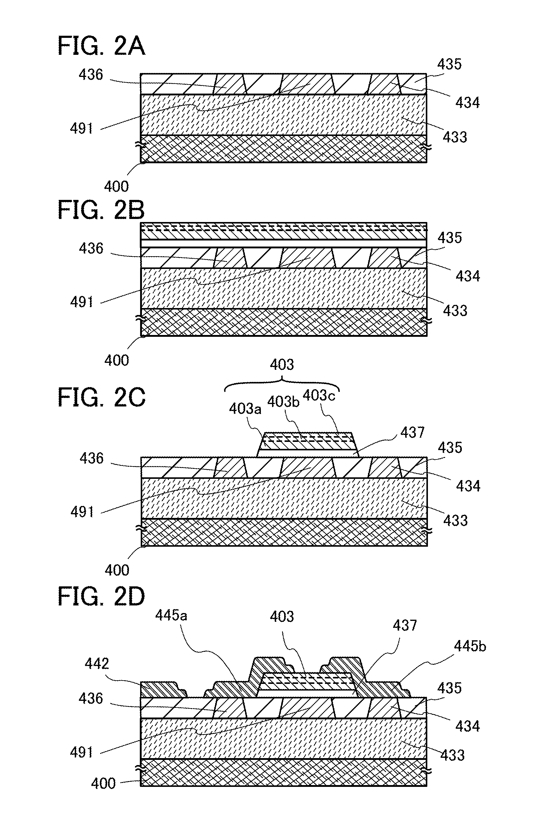
[0108]In this embodiment, one embodiment of a semiconductor device and one embodiment of a method for manufacturing the semiconductor device will be described with reference to FIGS. 2A to 2D. In this embodiment, an example of a method for manufacturing a transistor including an oxide semiconductor film is described.
[0109]First, an insulating film 433 is formed over a substrate 400 having an insulating surface and a conductive film is formed thereover by a sputtering method, an evaporation method, or the like. The conductive film is etched so that a conductive layer 491 and wiring layers 434 and 436 are formed.
[0110]There is no particular limitation on a substrate that can be used as the substrate 400 having an insulating surface as long as it has heat resistance enough to withstand heat treatment performed later. For example, a glass substrate of barium borosilicate glass, aluminoborosilicate glass, or the like, a ceramic substrate, a quartz substrate, or a sapphire substrate can b...
embodiment 2
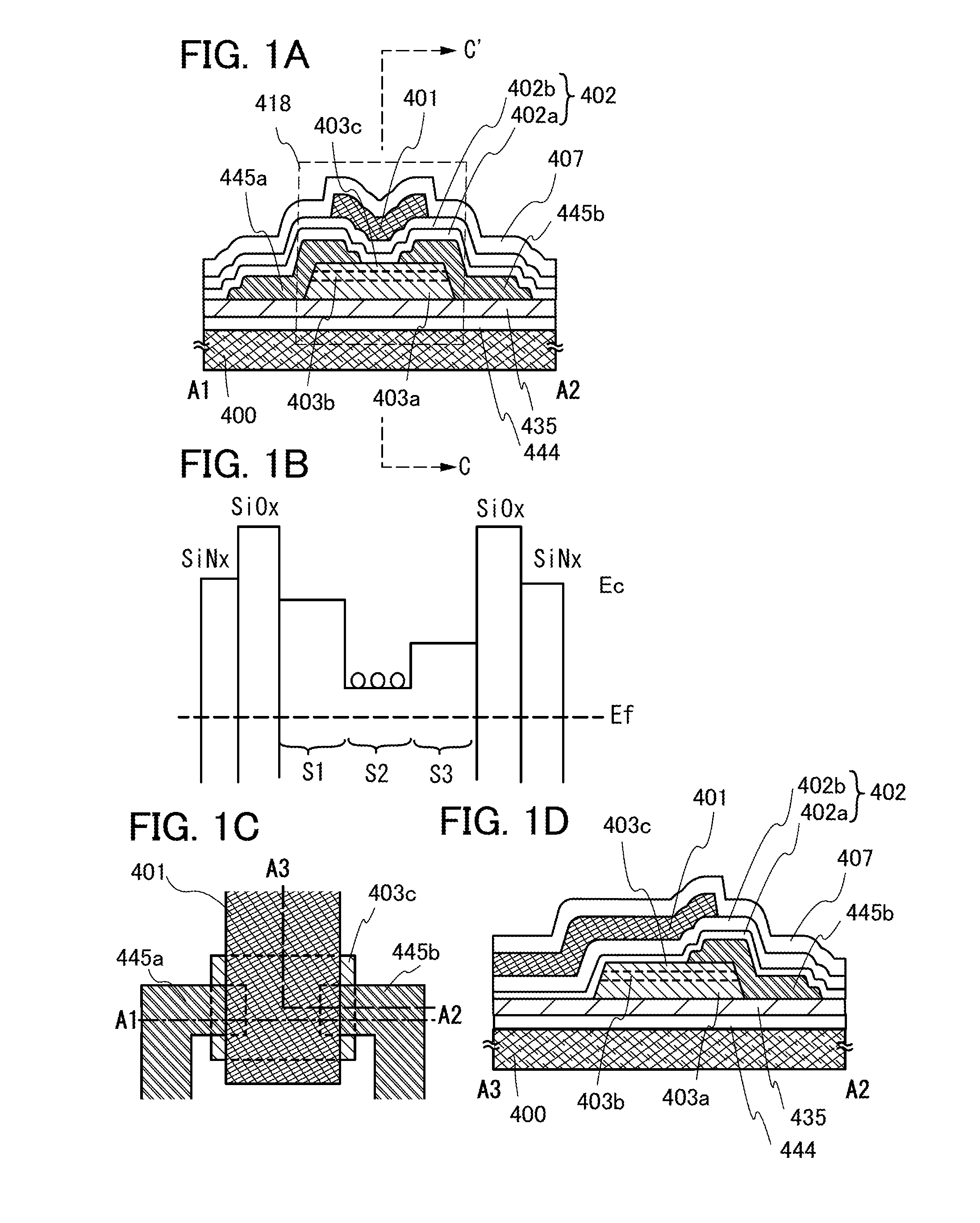
[0146]In this embodiment, a structural example in FIG. 4A which is partly different from the structure of FIG. 1A and a manufacturing method thereof are described below.
[0147]First, over the substrate 400, the oxide insulating film 435 is formed. The oxide insulating film 435 can be formed by a plasma CVD method, a sputtering method, or the like, using silicon oxide, silicon oxynitride, aluminum oxide, aluminum oxynitride, hafnium oxide, gallium oxide, gallium oxide zinc, zinc oxide, or a mixed material of any of these materials. The oxide insulating film 435 may have either a single-layer structure or a stacked-layer structure. If needed, a nitride insulating film such as a silicon nitride film may be provided between the substrate 400 and the oxide insulating film 435.
[0148]Next, the first oxide semiconductor film 403a and the second oxide semiconductor film 403b are formed by patterning using the same mask, and then the third oxide semiconductor film 403c is formed. Since the thi...
embodiment 3
[0154]In this embodiment, an example of a semiconductor device including the transistor described in Embodiment 1 is described with reference to FIGS. 5A and 5B.
[0155]The semiconductor device illustrated in FIGS. 5A and 5B includes transistors 740 and 750 including a first semiconductor material in a lower portion, and a transistor 610 including a second semiconductor material in an upper portion. The transistor 610 has the same structure as the transistor 415 described in Embodiment 1. The same reference numerals are used for the same parts as those in FIGS. 3A and 3B. FIG. 5B is a circuit diagram of the semiconductor device in FIG. 5A.
[0156]Here, the first semiconductor material and the second semiconductor material are preferably materials having different band gaps. For example, the first semiconductor material may be a semiconductor material other than an oxide semiconductor (e.g., silicon) and the second semiconductor material may be an oxide semiconductor. A transistor includ...
PUM
 Abstract
Description
Claims
Application Information