Method of manufacturing semiconductor device, method of processing substrate and substrate processing apparatus

a technology of semiconductor devices and processing equipment, applied in the direction of coatings, chemical vapor deposition coatings, metallic material coating processes, etc., can solve the problems of difficult reduction of hydrogen, restriction of film thickness uniformity and step coverage properties, and high defect density of sin film, etc., to achieve low hydrogen concentration in film, good uniformity in film thickness, and high resistance to stress voltage

Active Publication Date: 2013-12-19
KOKUSA ELECTRIC CO LTD
View PDF8 Cites 21 Cited by
  • Summary
  • Abstract
  • Description
  • Claims
  • Application Information

AI Technical Summary

Benefits of technology

[0038]According to the present invention, there is provided a method of manufacturing a semiconductor device, a method of processing a substrate and a substrate processing apparatus, capable of forming an insulating film with high resistance to a stress voltage, with extremely low hydrogen concentration in a film, and good uniformity in a film thickness, in a high temperature zone.

Problems solved by technology

However, the SiN film has a high defect density, and a reduction thereof is requested.
Further, in the CVD method, it is difficult to reduce the hydrogen by setting a film formation temperature to be high, under restriction of film thickness uniformity and step coverage properties.

Method used


Image

  • Method of manufacturing semiconductor device, method of processing substrate and substrate processing apparatus
  • Method of manufacturing semiconductor device, method of processing substrate and substrate processing apparatus
  • Method of manufacturing semiconductor device, method of processing substrate and substrate processing apparatus

Examples


first example

[0154]Next, a first example will be described.

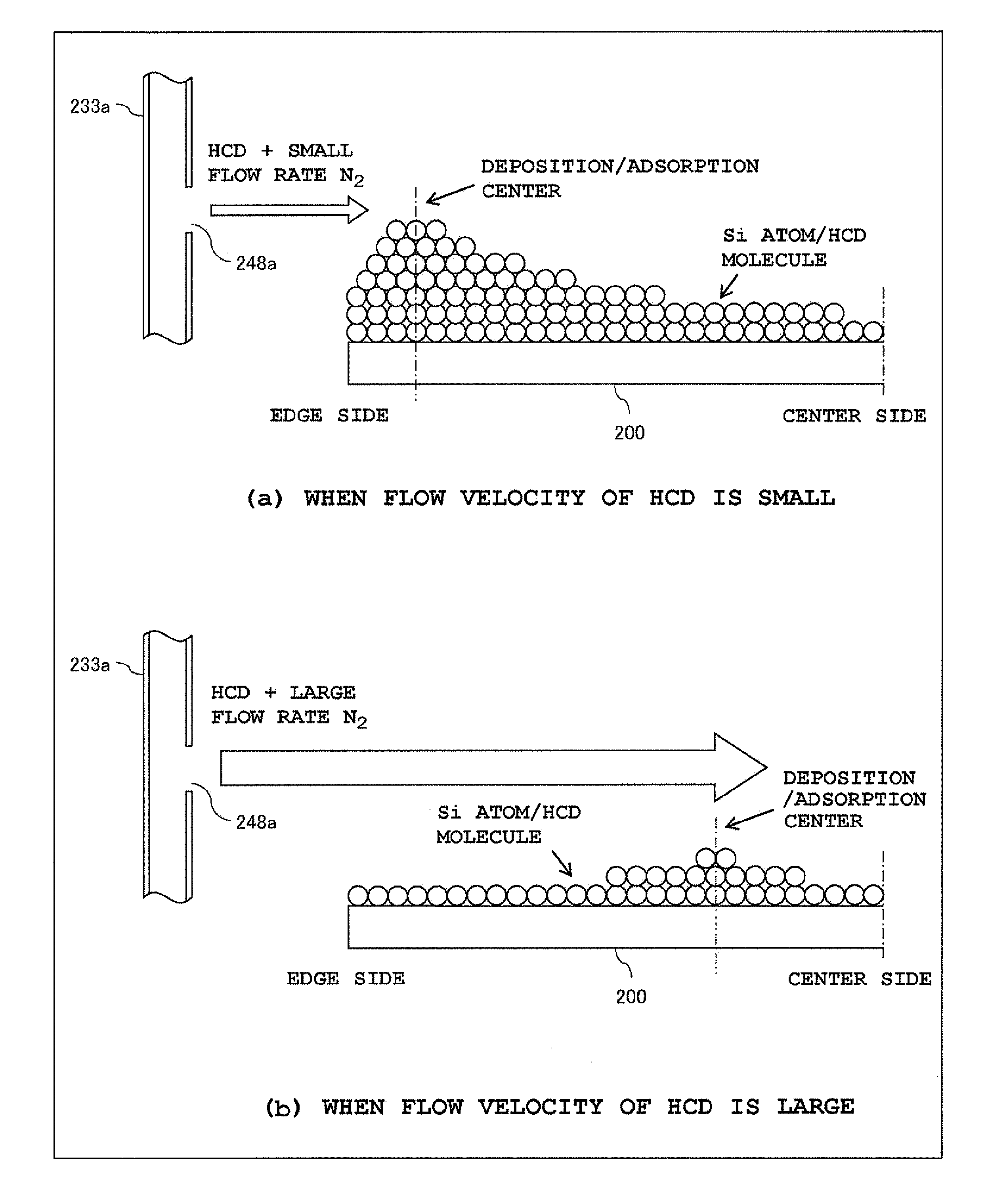
[0155]The SiN film was formed on the wafer by repeating the cycle of steps 1 to 4 in the film formation sequence of the above-mentioned embodiment as one cycle, and the film thickness and the uniformity of the film thickness in the wafer plane was measured. A film formation temperature (wafer temperature) was set to the temperature in a range of 800 to 950° C. where the uniformity of the film thickness was deteriorated remarkably. The supply flow rate of the N2 gas as the deposition / adsorption inhibiting gas is varied in three ways in a range of 2 to 8 slm. Such three ways of the supply flow rate of the N2 gas was expressed by a ratio of (A) 2.5, (B) 5.0, (C) 7.5, with a certain flow rate value as a reference, namely, 1, each of them called flow rate condition (A), flow rate condition (B), and flow rate condition (C), respectively. The condition in the range of the processing condition described in the above-mentioned embodiment is used ...

second example

[0161]Next, explanation is given for a second example.

[0162]The SiN film was formed on the wafer by repeating a cycle of steps 1 to 4 in the film formation sequence of the above-mentioned embodiment, with this sequence as one cycle, and a hydrogen concentration and a film density of the formed SiN film were measured. The film formation temperature (wafer temperature) was varied in three ways in a range of 600° C. to 900° C. The supply flow rate of the N2 gas as the deposition / adsorption inhibiting gas was set to a certain flow rate in a range of 2 to 8 slm. The condition in the range of the processing condition described in the above-mentioned embodiment, was used as the other processing condition (processing condition in each step). Further, the hydrogen concentration of the SiN film was measured by TDS (Thermal Desorption Spectroscopy), and the film density was measured by SRP (X-ray Reflection). Results thereof are shown in FIG. 10 and FIG. 11.

[0163]FIG. 10 is a view showing a re...

third example

[0168]Next, a third example will be described.

[0169]The SiN film was formed on the wafer based on the film formation sequence of this embodiment in a case of using the deposition / adsorption inhibiting gas, and the film formation sequence of this embodiment in a case of not using the deposition / adsorption inhibiting gas, and the uniformity of the film thickness in the wafer plane of the SiN film was respectively measured. The SiN film was formed by repeating a cycle of steps 1 to 4 in the film formation sequence of the above-mentioned embodiment, with these steps as one cycle. The film formation temperature in the film formation sequence of this embodiment in the case of using the deposition / adsorption inhibiting gas was varied in a range of 800 to 900° C. The film formation temperature in the film formation sequence of this embodiment in the case of not using the deposition / adsorption inhibiting gas was varied in a range of 600 to 900° C. The condition in the range of the condition ...


PUM

PropertyMeasurementUnit
temperatureaaaaaaaaaa

Abstract

Provided: forming a specific element-containing layer by supplying a source gas to the substrate heated in a processing vessel, under a condition that a thermal decomposition reaction of the source gas is caused; changing the specific element-containing layer to a nitride layer by supplying a nitrogen-containing gas to the substrate; and changing the nitride layer to an oxynitride layer by supplying an oxygen-containing gas to the substrate, the source gas is sprayed in parallel to a surface of the substrate more strongly than a case of spraying the inert gas in parallel to the surface of the substrate in purging the inside of the processing vessel, by supplying an inert gas or a hydrogen-containing gas through the nozzle.

Description

TECHNICAL FIELD[0001]The present invention relates to a method of manufacturing a semiconductor device and a method of processing a substrate including a step of forming a thin film on a substrate, and a substrate processing apparatus suitably used in the step.DESCRIPTION OF RELATED ART[0002]A flush memory includes an electronic storage region (floating gate) surrounded by an insulating film, and has an operation principle in which information is written by exchange of electrons through a thin tunnel oxide film, and the electrons are held and stored for a long time by utilizing insulation properties of the thin oxide film. In the flash memory, the electrons or holes (positive holes) are passed through the tunnel insulating film and accumulated in the floating gate, during write and erase of the information, to thereby store the information. However, as a miniaturization is in progress, a thinner Equivalent Oxide Thickness (EOT) in the tunnel insulating film is requested. Therefore, ...

Claims


Application Information

Patent Timeline
Patent Type & Authority Applications(United States)
IPC IPC(8): H01L21/02
CPCH01L21/0214C23C16/308C23C16/45527H01L21/0228H01L21/0217H01L21/02211C23C16/45531C23C16/45563H01L21/02247
Inventor OTA, YOSUKEHIROSE, YOSHIROAKAE, NAONORITAKASAWA, YUSHIN
Owner KOKUSA ELECTRIC CO LTD
Why Eureka
Try Eureka