Lateral electrochemical etching of iii-nitride materials for microfabrication

a technology of iiinitride and electrochemical etching, which is applied in the direction of lasers, semiconductor lasers, solid-state devices, etc., can solve the problems of difficult to match the cavity mode with the emission wavelength of the active layer, and the structure is difficult to produce, so as to achieve high selective material conductivity

Active Publication Date: 2014-01-02
YALE UNIV
View PDF24 Cites 54 Cited by
  • Summary
  • Abstract
  • Description
  • Claims
  • Application Information

AI Technical Summary

Benefits of technology

[0010]The described technology relates to methods and structures for lateral electrochemical etching of III-nitride materials to produce optically smooth surfaces, and for controllably forming porous III-nitride material. The etching processes are compatible with InGaN based light emitters and integrated devices. The etching techniques may be used for manufacturing various microstructures and microdevices. For example, the etching techniques may be used for making vertical cavity surface emitting lasers (VCSELs) that include distributed Bragg reflector (DBR) structures. According to some embodiments, the VCSELs and DBR structures comprise III-nitride semiconductor materials that may be deposited in multiple layers on a substrate, and the formed DBR structure comprises a limited number of alternating III-nitride / air layers. In various embodiments, the electrochemical etching of a DBR structure laterally removes alternating layers in a multilayer structure, and leaves optically smooth air / semiconductor interfaces. The electrochemical etching may be highly selective to the conductivity of the materials. The conductivity (and resulting etching properties) may be controlled by doping the materials during their deposition. By modulating the doping of epitaxial layers, highly-doped n-type layers may be laterally etched over large distances (>10 microns) in confined regions (<500 nm layer thickness sandwiched between non-etched layers) at high etch rates (>5 microns / min). The etching techniques may be used to fabricate other III-nitride devices, e.g., LEDs, high electron mobility transistors, high-power tranistors, and MEMs devices

Problems solved by technology

However, these structures are difficult to produce and do not exhibit high refractive index contrast between the alternating layers.
Additionally, it is difficult to match the cavity mode with an active layer emission wavelength.
However, this approach is complex to implement and suffers from low yield during manufacture.
However, challenges still exist in both approaches toward ultimate manufacturability.
Such a thick DBR structure causes a narrow stopband (<50 nm), creates issues in stress management on the device, and reduces the benefit of the Purcell effect.
The membrane structures prepared by the two techniques generally suffer from etched surface roughness that contributes to scattering losses in the optical devices.

Method used


Image

  • Lateral electrochemical etching of iii-nitride materials for microfabrication
  • Lateral electrochemical etching of iii-nitride materials for microfabrication
  • Lateral electrochemical etching of iii-nitride materials for microfabrication

Examples


example 1

Controlled Porosification of GaN

[0067]This example describes the use of hydrofluoric acid (HF) as a versatile electrolyte for preparing porous GaN with a wide range of morphology from curved to highly parallel pores. The interplay among different electro-chemical processes may be elucidated using cyclic voltammetry. Under suitable conditions, a record-high rate of porosification (up to 150 μm / min) is observed. The influence of electrolyte concentration, sample conductivity (doping), and anodization potential is investigated. The rich variety of pore morphology can be explained by a depletion-region model where the available current flow pathways in GaN, determined by the ratio of inter-pore spacing and the width of depletion region, define the directions of pore propagation and branching.

[0068]Electrochemical porosification experiments were conducted in a two-electrode cell at room temperature with n-type GaN as the anode and a platinum wire as the counter electrode (cathode). Ga-po...

example 2

Fabrication of a MQW / Air-Semiconductor DBR Structure

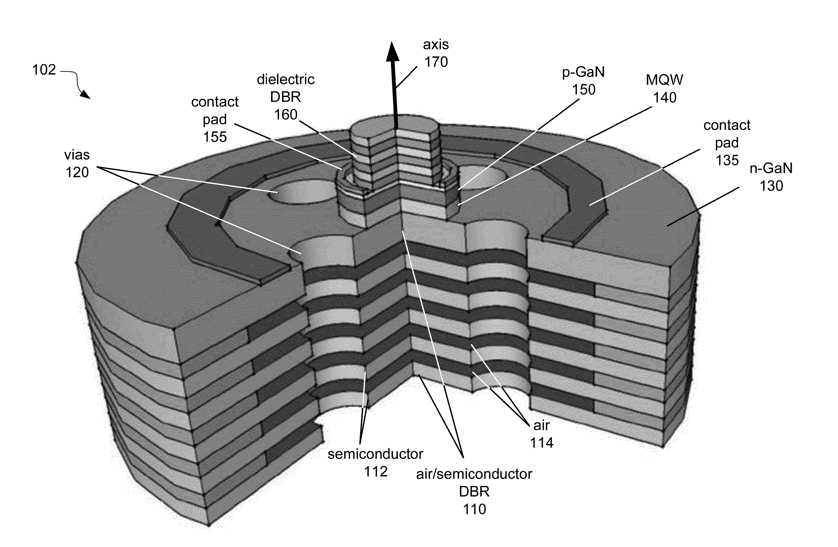
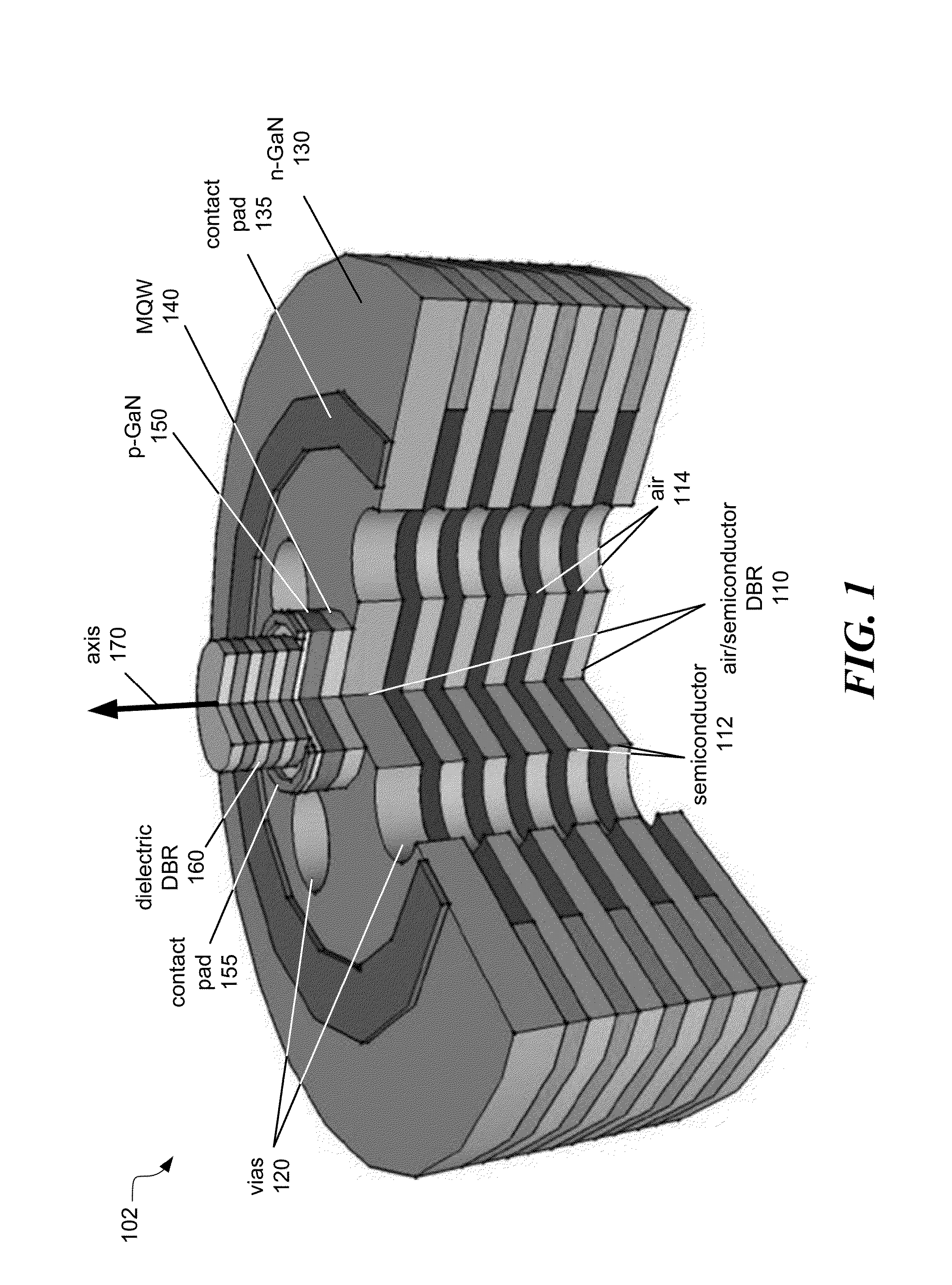
[0083]This example describes in further detail the fabrication of a membrane-based GaN / air-gap DBR for blue / green light emitting devices. The formation of membrane DBRs and microcavities may employ electrochemical etching described above in which selective lateral etching of layers is achieved by adjusting the conductivity of layers rather than chemical composition. This can relieve greatly the burden in creating epitaxial DBRs. The lateral-etching process is found to be compatible with InGaN based light emitters.

[0084]The emission of InGaN multiple quantum wells (MQWs) was modified successively with the formation of a DBR underneath the MQW and the capping of the MQW with a silver top mirror. Micro-reflectance measurements of a fabricated DBR structure shows over 98% peak reflectance and a wide stopband (over 150 nm) with only four pairs of GaN / air-gap layers. Micro-photoluminescence spectra of InGaN multiple quantum wells (MQWs) ...


PUM


Abstract

Conductivity-selective lateral etching of III-nitride materials is described. Methods and structures for making vertical cavity surface emitting lasers with distributed Bragg reflectors via electrochemical etching are described. Layer-selective, lateral electrochemical etching of multi-layer stacks is employed to form semiconductor/air DBR structures adjacent active multiple quantum well regions of the lasers. The electrochemical etching techniques are suitable for high-volume production of lasers and other III-nitride devices, such as lasers, HEMT transistors, power transistors, MEMs structures, and LEDs.

Description

RELATED APPLICATIONS[0001]This application claims the benefit of U.S. provisional application Ser. No. 61 / 665,617 titled “III-Nitride Vertical Cavity Surface Emitting Lasers (VCSEL) with GaN / air DBR by Electrochemical Etching,” filed on Jun. 28, 2012, which is incorporated herein by reference in its entirety.BACKGROUND[0002]1. Technical Field[0003]The technology relates to methods and structures for performing etching of sacrificial layers of III-nitride material. The etching techniques may be used for micro- and nano-fabrication of integrated devices, such as vertical cavity surface emitting lasers (VCSELs) based on III-nitride semiconductor material. The VCSELs may include air / semiconductor, distributed Bragg reflector (DBR) structures formed adjacent to the VCSEL using lateral, electrochemical etching techniques.[0004]2. Discussion of the Related Art[0005]The etching of semiconductor materials is an important technique that is used in microfabrication processes. Various kinds of ...

Claims


Application Information

Patent Timeline
Patent Type & Authority Applications(United States)
IPC IPC(8): H01L21/306H01L33/00H01S5/343
CPCH01L33/0075H01S5/343H01L21/30612B82Y20/00H01L21/306H01L21/30635H01L33/105H01L2924/0002H01S5/18341H01S5/18363H01S5/18369H01S5/34333H01S5/187H01L2924/00
Inventor HAN, JUNG
Owner YALE UNIV
Why Eureka
Try Eureka