
Method of manufacturing semiconductor device

a manufacturing method and semiconductor technology, applied in semiconductor devices, semiconductor/solid-state device testing/measurement, electrical equipment, etc., can solve problems such as many new difficulties and challenges, device failure, and reduced yield, so as to reduce process complexity, optimize threshold voltage, and reduce damage to the substrate

Active Publication Date: 2014-01-09
INST OF MICROELECTRONICS CHINESE ACAD OF SCI
View PDF3 Cites 6 Cited by
  • Summary
  • Abstract
  • Description
  • Claims
  • Application Information

AI Technical Summary

Benefits of technology

The present patent aims to provide a new method for etching a spacer that reduces damage to the substrate, reduces EOT and enhances gate control capability and driving current. This is achieved by using a dual-layer complex spacer and performing two etching operations with helium gas. The method simplifies the process, optimizes threshold voltage, reduces process complexity, and improves overall performance.

Problems solved by technology

In manufacture of Large Scale Integrated Circuits, generally a dielectric spacer is formed before a Light Doped Drain (LDD) implantation process, to prevent source / drain implantation at a greater dose from being too close to a channel to cause source-drain punch-through, which in turn results in device failure and a reduced yield.
Further, the gate last process is becoming a dominant one because of its good control of thermal effects and threshold voltages, but causes many new difficulties and challenges.
This tends to deteriorate the uniformity of the etching rate of the spacer.
Especially, current spacer etching techniques are generally based on Ar-based gases, which tend to make damages to the substrate, particularly for nanometer-scale devices.
Especially, when the liner layer of silicon oxide over the gate is very thin, it is easy for oxygen plasma to penetrate through the thin oxide layer to react with the substrate, resulting in a great silicon loss.

Method used


Image

  • Method of manufacturing semiconductor device
  • Method of manufacturing semiconductor device
  • Method of manufacturing semiconductor device

Examples


Embodiment Construction

[0030]Hereinafter, exemplary embodiments of the present disclosure will be described in detail with reference to attached drawings. It is to be noted that like symbols denote like structures throughout the drawings. Here, terms, such as “first,”“second,”“on,”“below,”“thick,” and “thin,” are used to describe various device structures. However, such descriptions are not intended to imply relationships of the described device structures in terms of space, order or layer-level, unless otherwise indicated.

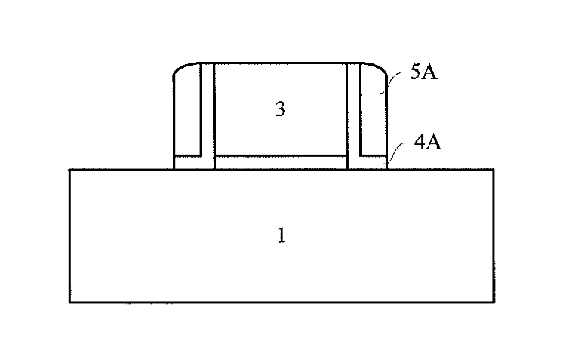
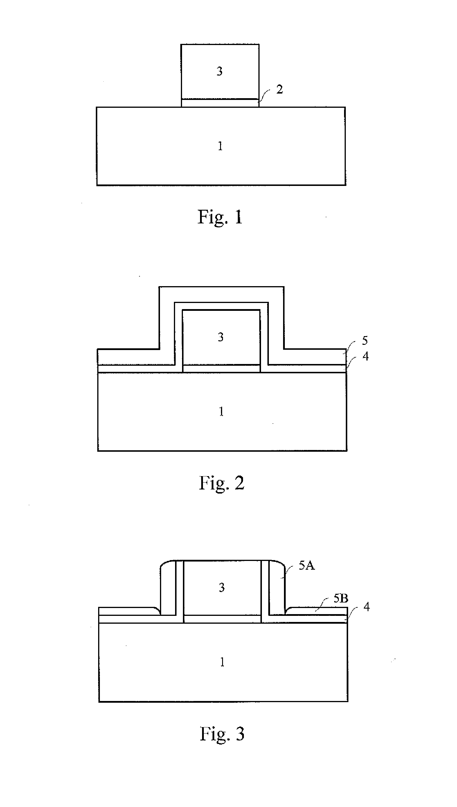
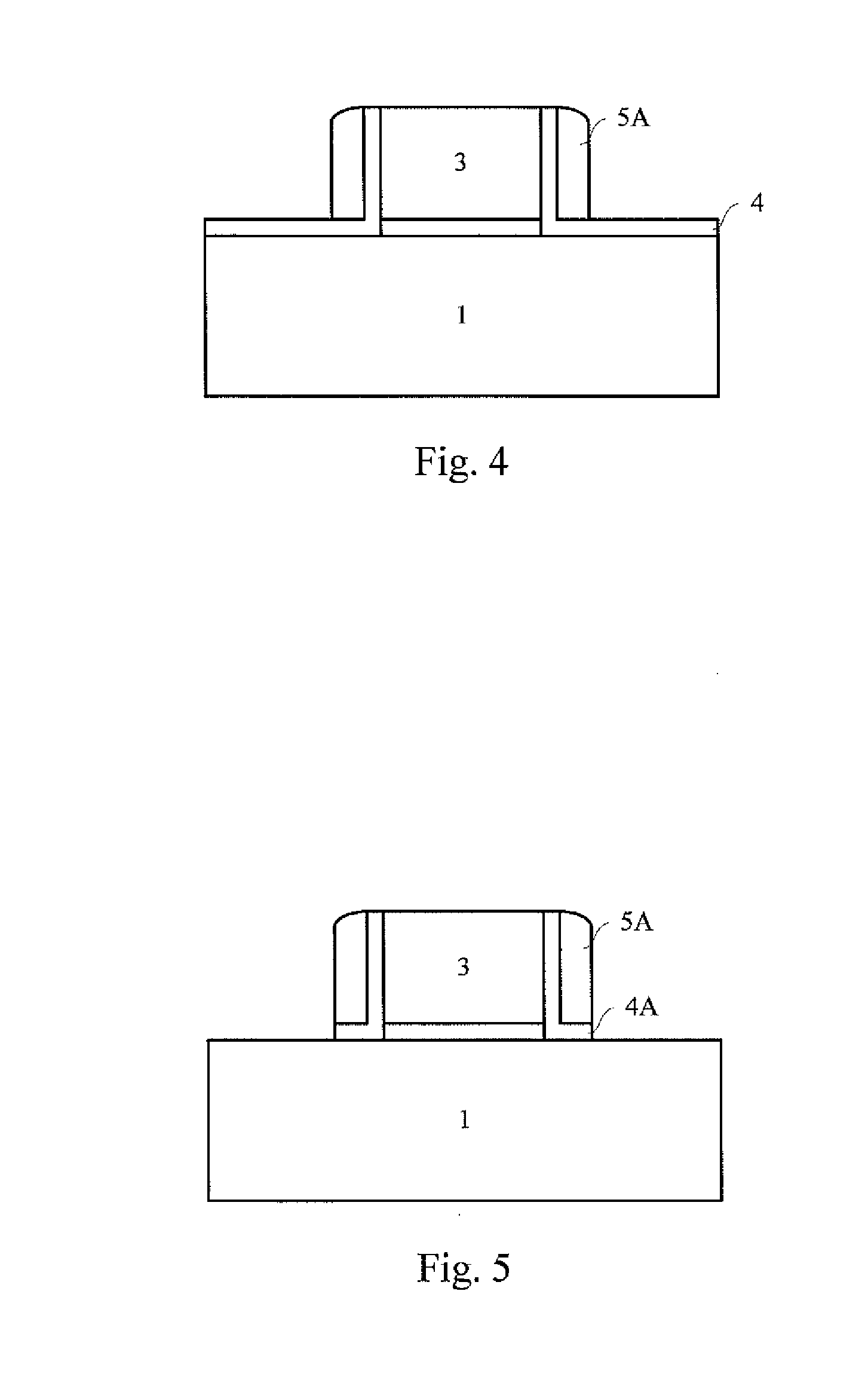
[0031]Referring to FIG. 6 and FIG. 1, at S601, a gate stack is formed on a substrate. The gate stack can be one for a gate first process or for a gate last process. The substrate 1 is provided, and may comprise bulk Si, SOI, bulk Ge, GeOI, SiGe, GeSb, or a group III-V or group II-VI compound semiconductor substrate, such as GaAs, GaN, InP, and InSb. To be compatible with the existing CMOS processes and applicable to manufacture of large scale digital integrated circuits, the substrate 1...


PUM

PropertyMeasurementUnit
thicknessaaaaaaaaaa
angleaaaaaaaaaa
angleaaaaaaaaaa

Abstract

A method of manufacturing a semiconductor device is disclosed. The method may comprise: forming a gate stack on a substrate; depositing a first dielectric layer and a second dielectric layer sequentially on the substrate and the gate stack; and etching the second dielectric layer and the first dielectric layer sequentially with an etching gas containing helium to form a second spacer and a first spacer, respectively. According to the method disclosed herein, a dual-layer complex spacer configuration is achieved, and two etching operations where the etching gas comprises the helium gas are performed. As a result, it is possible to reduce damages to the substrate and also to reduce the process complexity. Further, it is possible to optimize a threshold voltage, effectively reduce an EOT, and enhance a gate control capability and a driving current.

Description

CROSS-REFERENCE TO RELATED APPLICATION(S)[0001]The present application claims priority to Chinese Application No. 201210229524.9, entitled “METHOD OF MANUFACTURING SEMICONDUCTOR DEVICE,” filed on Jul. 3, 2012, which is incorporated herein by reference in its entirety.TECHNICAL FIELD[0002]The present disclosure relates to the field of manufacture of semiconductor integrated circuits, and particularly, to a method of etching a spacer.BACKGROUND[0003]In manufacture of Large Scale Integrated Circuits, generally a dielectric spacer is formed before a Light Doped Drain (LDD) implantation process, to prevent source / drain implantation at a greater dose from being too close to a channel to cause source-drain punch-through, which in turn results in device failure and a reduced yield.[0004]Presently, a popular 65 nm node spacer or even a 45 nm node spacer can be fabricated as follows. Before the LDD implantation process, a thin film layer of silicon oxide is deposited or thermally grown. For e...

Claims


Application Information

Patent Timeline
Patent Type & Authority Applications(United States)
IPC IPC(8): H01L29/66
CPCH01L29/66477H01L22/26H01L29/66545H01L29/6656H01L21/31116
Inventor MENG, LINGKUAN
Owner INST OF MICROELECTRONICS CHINESE ACAD OF SCI
Learn More