LED epitaxial Structure

a technology of epitaxial structure and led to, which is applied in the direction of electrical apparatus, semiconductor/solid-state device manufacturing, and semiconductor devices. it can solve the problems of poor cooling capacity, low cost, and cost increase, and achieve good lattice matching, heat dissipation, and light-emitting efficiency. the effect of good improvemen

Inactive Publication Date: 2014-02-06
NAT CHUNG SHAN INST SCI & TECH
View PDF3 Cites 1 Cited by
  • Summary
  • Abstract
  • Description
  • Claims
  • Application Information

AI Technical Summary

Benefits of technology

[0012]In addition, the third layer thin film of a single crystal gallium nitride is epitaxially grown on the second layer thin film of the single crystal aluminum nitride via another epitaxial process, operating as a light emitting layer. Because both the thermal expansion coefficients and the lattice constants of the aluminum nitride materials and the gallium nitride materials are quite close to each other, which allows the second layer thin film of the single crystal aluminum nitride and the third layer thin film of a single crystal gallium nitride to have a good lattice match and allow the heat dissipation, lifespan and light emitting efficiency of the LED to achieve good improvements.

Problems solved by technology

(due to differences between TE, problems arise)
Comparatively speaking, Sapphire substrate has a lower cost, but poor cooling capacity (about 40 W / mK), which needs flip-chip process or other special process to improve the cooling capacity, resulting in the increment of costs.
Moreover, the lattice and thermal expansion match of the sapphire and gallium nitride (GaN) are poor, and the lattice constant between the c-cut sapphire and gallium nitride is about 15% to 30% mismatch, leading to the decrease of epitaxial quality of the gallium nitride.
However, since the cost of SiC substrate is high, the general LED epitaxial plants still use sapphire as the substrate for epitaxial growth.

Method used


Image

  • LED epitaxial Structure
  • LED epitaxial Structure
  • LED epitaxial Structure

Examples


Embodiment Construction

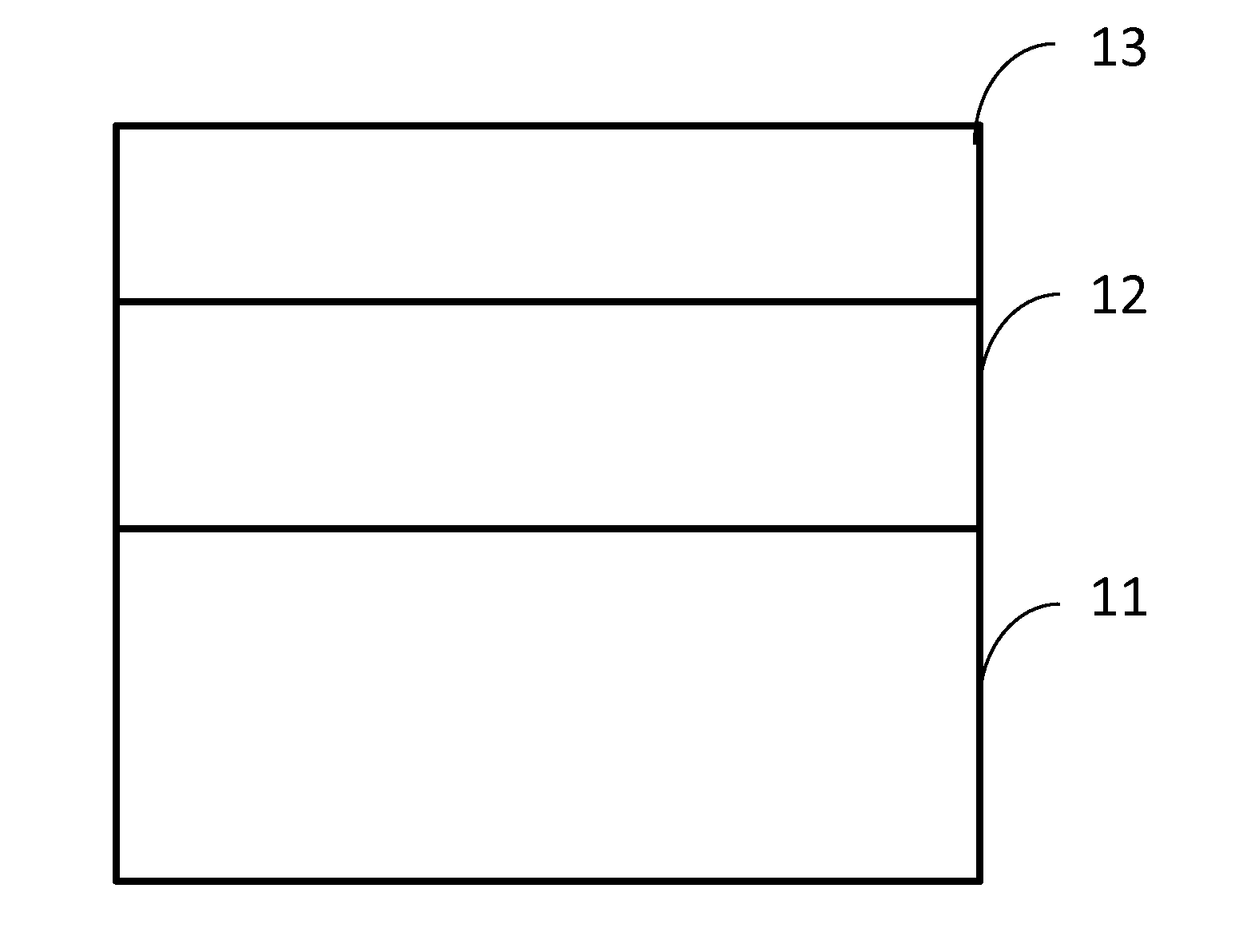
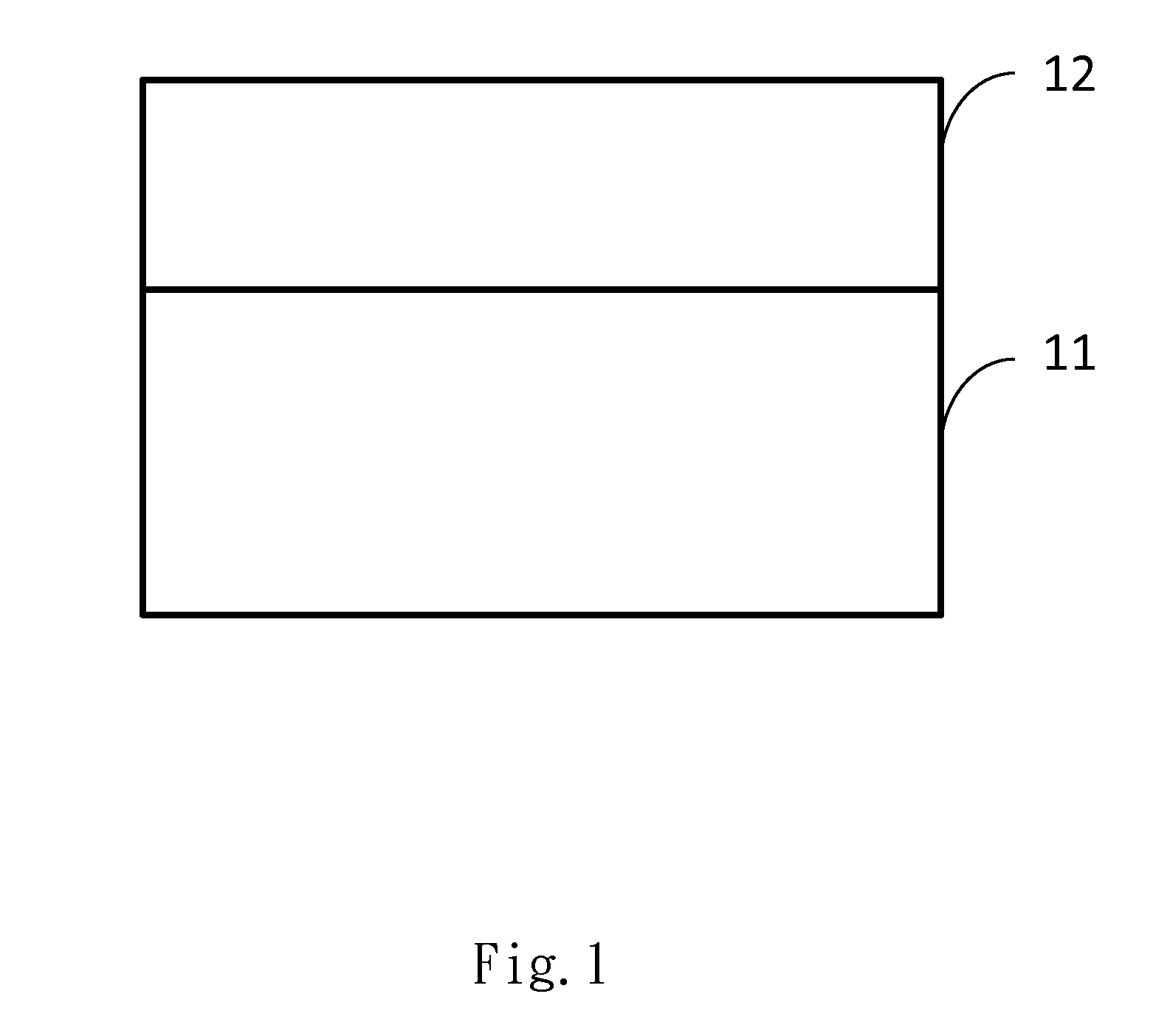
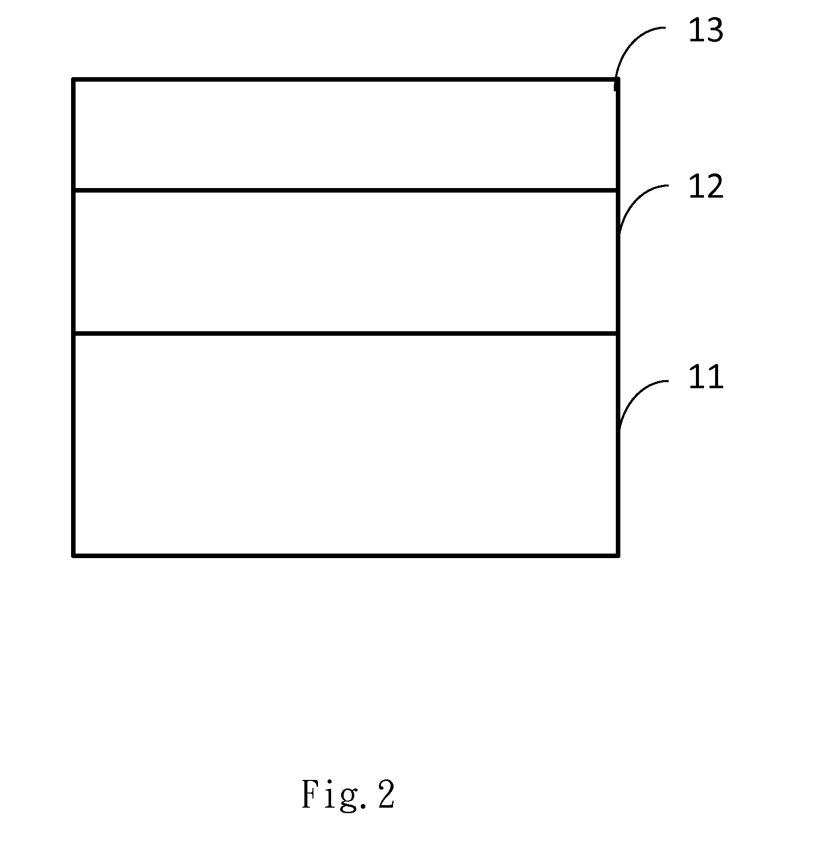
[0016]With reference to FIG. 1, the LED epitaxial structure provided by the embodiment of the present invention is an epitaxial substrate, which is composed of a first layer thin film 11 and a second layer thin film 12.

[0017]First of all, the first layer thin film 11 is used as a substrate and an epitaxial process is processed on one side of the first layer thin film 11. An organometallic compound is converted into the second layer thin film 12 on the side of the first layer thin film 11 via chemical reactions in the epitaxial process of metal organic chemical vapor deposition (MOCVD).

[0018]The first layer thin film 11 is a polycrystalline aluminum nitride thin film; the second layer thin film 12 is a single crystal aluminum nitride thin film.

[0019]Because the aluminum nitride has the advantages of wide energy band gap (6.2 eV), high thermal conductivity (320 W / mK), good electrical insulation, high mechanical strength and chemical stability, and there are good lattice and thermal ex...


PUM

PropertyMeasurementUnit
epitaxial structureaaaaaaaaaa
structureaaaaaaaaaa
energy band gapaaaaaaaaaa

Abstract

An LED epitaxial structure includes the first layer thin film and the second layer thin film. The first layer thin film and the second layer thin film are polycrystalline aluminum nitride and single crystal aluminum nitride respectively, which have good thermal conductivity, insulation, mechanical intensity, and chemistry stability. Based on the substrate mentioned above, growing a single crystal gallium nitride on the second layer thin film as the third layer thin film allows the single crystal aluminum nitride and gallium nitride to have good lattice and thermal expansion match, resulting in the promotion of light emitting and thermal conduction efficiency.

Description

BACKGROUND OF THE INVENTION[0001]1. Field of the invention[0002]The present invention relates to an LED epitaxial structure, in particular, to a substrate material used for the epitaxial structure in the LED manufacturing process.[0003]2. Description of Related Art[0004]Regarding the LED light emitting device structure, substrate selection has a considerable influence on the characteristics and performance of the epitaxial wafer, such as: brightness, luminous efficiency and component lifespan, which are due to the lattice and thermal expansion differences between substrate and epitaxial materials. (due to differences between TE, problems arise)[0005]The substrate materials currently used in the general blue LED are sapphire (Al2O3) and silicon carbide (SiC).[0006]Comparatively speaking, Sapphire substrate has a lower cost, but poor cooling capacity (about 40 W / mK), which needs flip-chip process or other special process to improve the cooling capacity, resulting in the increment of c...

Claims


Application Information

Patent Timeline
Patent Type & Authority Applications(United States)
IPC IPC(8): H01L33/16
CPCH01L33/12H01L33/16H01L33/32H01L21/02389H01L21/02458H01L21/0254
Inventor KUO, YANG-KUOHSIANG, CHIA-YIKU, HUNG-TAI
Owner NAT CHUNG SHAN INST SCI & TECH
Why Eureka
Try Eureka