Temperature sensor device and radiation thermometer using this device, production method of temperature sensor device, multi-layered thin film thermopile using photo-resist film and radiation thermometer using this thermopile, and production method of multi-layered thin film thermopile

Inactive Publication Date: 2014-02-06
HME +1
View PDF38 Cites 47 Cited by
  • Summary
  • Abstract
  • Description
  • Claims
  • Application Information

AI Technical Summary

Benefits of technology

[0089]A composite thermopile is formed by laminating k layered thin films with thermopiles while the isometric thin films are placed in the temperature sensing part in a temperature sensing device according to the present invention. This provides an advantage that the internal resistance becomes smaller in proportion to one squared kth part of that of the conventional thermopile formed on one layered thin film, and a temperature sensor device with large S/N ration can be obtained which has thermocouples with the same total number n as the conventional one.
[0090]A temperature sensor device according to the present invention can be used as one sheet of temperature sensing part by laminating a plurality of thin films made of inorganic or organic material wherein layered thermopiles are formed. And also a thermopile can be highly sensitive because larger output can be obtained when it is composed of more thermocouples for the same temperature difference ΔT between junctions. This provides an advantage that a temperature sensor device with high sensitivity and relatively low resistance can be provided by three dimensional expansion of a composite thermopile having totally n thermocouples by lamination.
[0091]It is preferable to form electrodes of layered thermopiles on the upper layered thin film around through-holes formed on the upper layered thin film in the temperature sensor device according to the present invention so that interlay

Problems solved by technology

High internal resistance r increases Johnson noise, which is not preferable for the application as a sensor.
However, there exist some problems in the technology disclosed by this invention which need to be improved for mass production.
For example, production method is complicated having processes such as a process to paste a plurality of PET films to form multi-layered thin films and a process to form through-holes to connect an upper layered thermopile with lower one, and silver paste needs to be unfavorably used for the connection.
Furthermore, it is also a problem in this technology, when an inorganic material other than photo-resist film is selected such as silicon oxide for the material of each layered thin film, that many

Method used


Image

  • Temperature sensor device and radiation thermometer using this device, production method of temperature sensor device, multi-layered thin film thermopile using photo-resist film and radiation thermometer using this thermopile, and production method of multi-layered thin film thermopile
  • Temperature sensor device and radiation thermometer using this device, production method of temperature sensor device, multi-layered thin film thermopile using photo-resist film and radiation thermometer using this thermopile, and production method of multi-layered thin film thermopile
  • Temperature sensor device and radiation thermometer using this device, production method of temperature sensor device, multi-layered thin film thermopile using photo-resist film and radiation thermometer using this thermopile, and production method of multi-layered thin film thermopile

Examples


embodiment 1

Preferred Embodiment 1

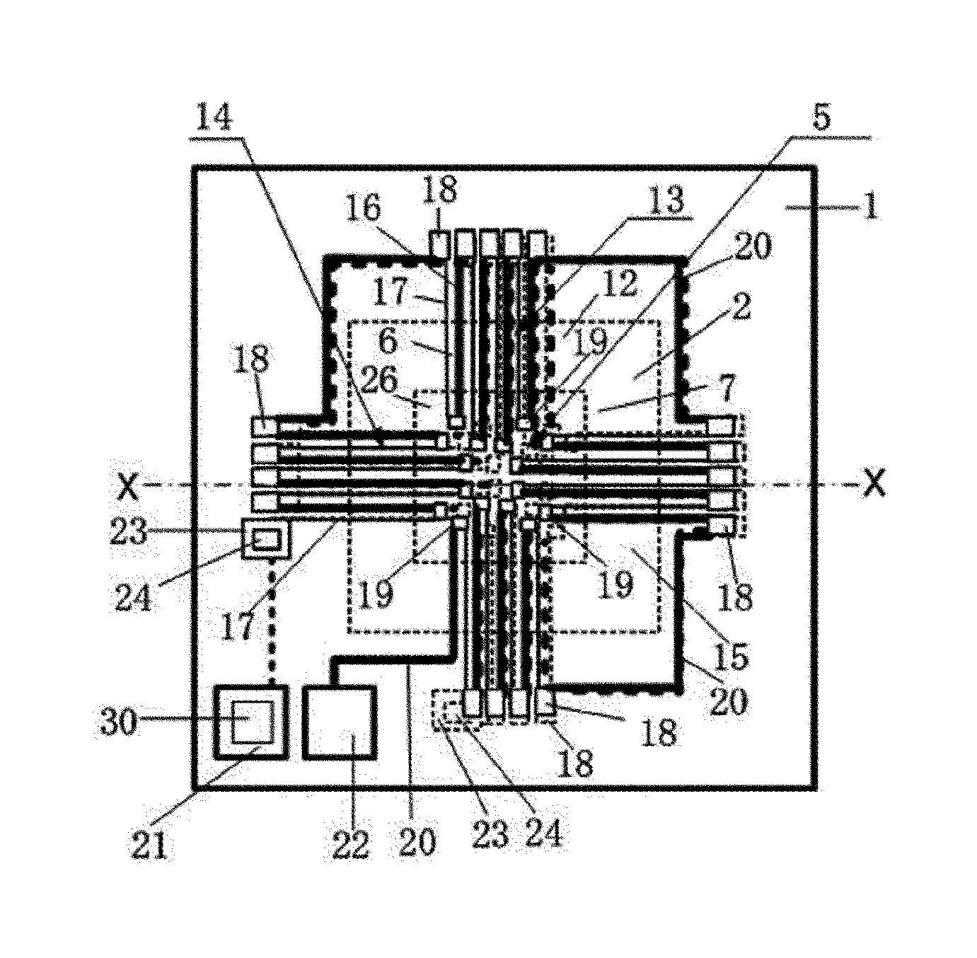
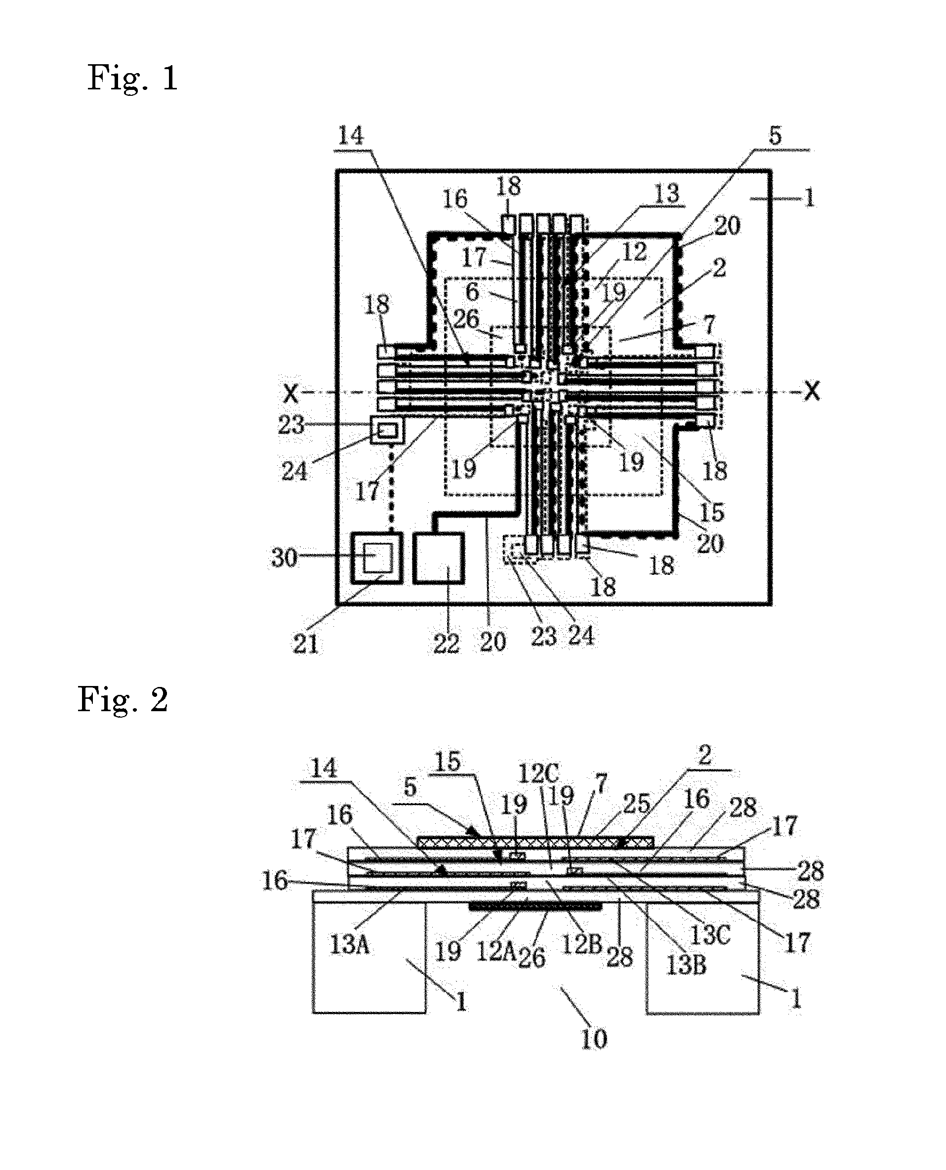
[0184]FIG. 1 is a plane view of an outline diagram to show an embodiment to explain the concept of a temperature sensor device according to the present invention applied for a thermal infrared sensor device, and FIG. 2 is a cross-sectional outline diagram along X-X line of the device shown in FIG. 1. FIG. 1 is a diagram when the device is applied for a thermal infrared sensor device. An infrared absorption film 25 and a thermal conduction thin film 26 formed on the light receiving part 7 are omitted in an easy-to-understand manner in the diagram. And also a thin film 2 is formed as a membrane (a diaphragm) on the substrate 1, being thermally isolated from the substrate by a cavity 10. A thermopile 3 is formed on the thin film 2. This thin film 2 is a multi-layered thin film 15 in the present invention and layered thermopiles 13 (13A, 13B, and 13C) are formed on each layered thin films 12 (12A, 12B, and 12C) which constitute this multi-layered thin film 15. The ...

embodiment 2

Preferred Embodiment 2

[0191]FIG. 4 is a plane view of an outline diagram of a structure to show an embodiment wherein a temperature sensor device according to the present invention is applied for an infrared sensor device using a thin film 2 as a temperature sensing part 5 at the light receiving part 7 made of inorganic material as explained in the aforementioned FIG. 2 and FIG. 3. In this embodiment, thin films 2A and 2B are formed as two temperature sensing parts 5A and 5B in the form of a cantilever in the same light receiving part 7. And composite thermopiles 14A and 14B are composed of multi-layered thin films 15A and 15B each having three-layered films. And multi-layered thin films 15A and 15B are composed of layered thermopiles 13 each having a layered thin film 12. For example, a p-n junction diode is formed on the substrate 1 as an absolute temperature sensor 34 to measure an absolute temperature of the substrate 1 as a reference temperature. The outputs of two different co...

embodiment 3

Preferred Embodiment 3

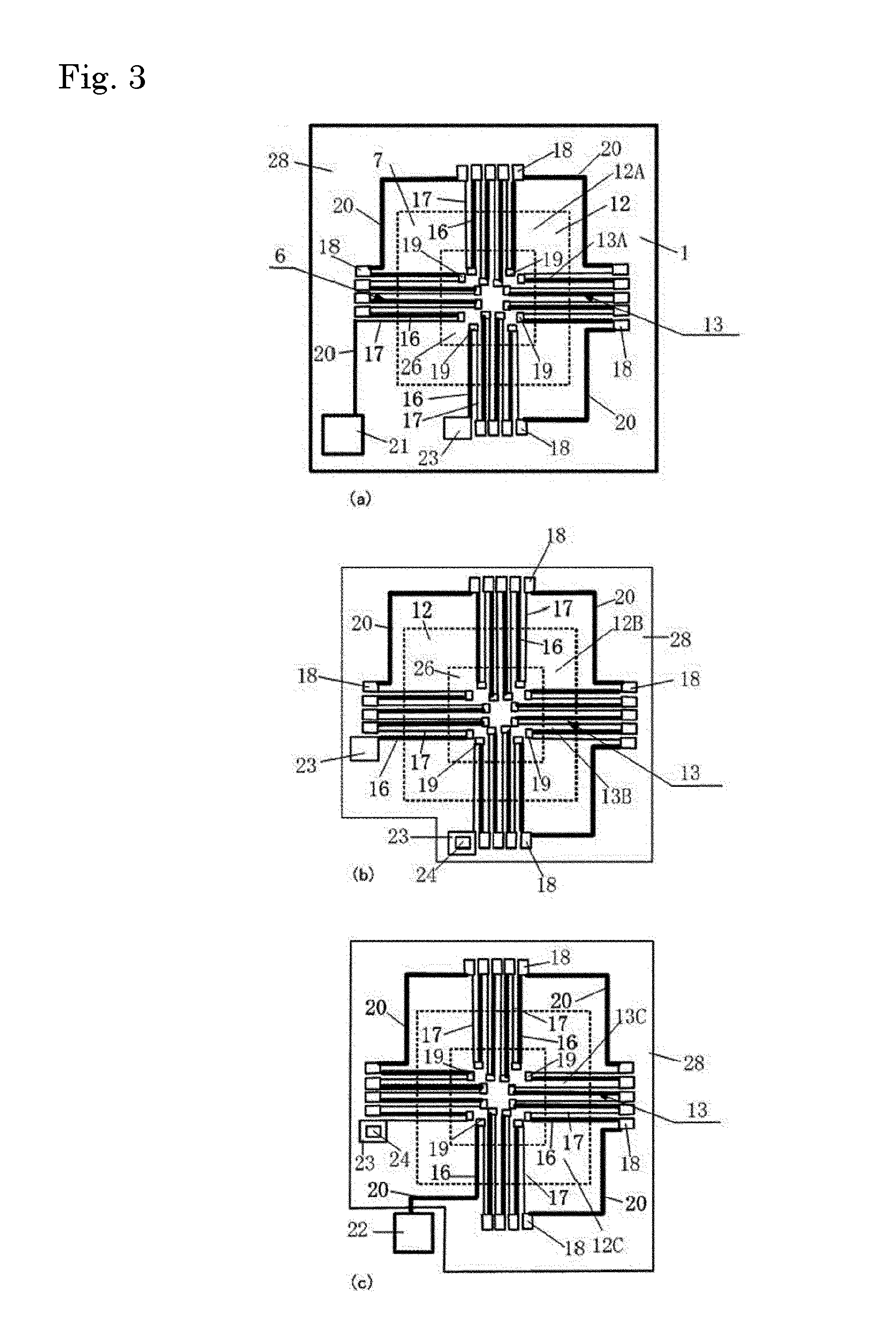
[0195]FIG. 5 is a diagram to show an embodiment of a thermal infrared sensor device wherein each layered thin films 12A, 12B, 12C are made of organic thin films in FIG. 5(a), FIG. 5(b), and FIG. 5(c) which are diagrams to show the patterns of three layered thin films 12A, 12B, 12C and their layered thermopiles 13A, 13B, 13C to explain a composite thermopile 14 by disassembling a temperature sensor device according to the present invention into layered thermopiles 13A, 13B, 13C which are formed on each layered thin films 12A, 12B, 12C which constitute the composite thermopile 14 with the multi-layered thin film 15 of the device. FIG. 6 is a cross-sectional view of an outline diagram of a temperature sensor device surrounded by an isolation region wherein a multi-layered thin film 15 is bonded with the substrate 1 by an epoxy type adhesive agent 27, wherein three layered thin films 12A, 12B, 12C with layered thermopiles 13A, 13B, 13C as shown in FIG. 5 are lamina...


PUM


Abstract

Disclosed are a temperature sensor device using a thermopile, the total number n of thermocouples thereon can be increased without greatly increasing the internal resistance of the thermopile r, providing high output level and high S/N ratio, a highly sensitive radiation thermometer using the device, and production method of the device using organic material for thin films to form the thermopile. These provide a standardized inexpensive multi-layered thin film thermopile, a radiation thermometer with high sensitivity, and production method of these devices. The temperature sensor device is a device wherein a thermopile which is formed on a thin film thermally isolated from a substrate is place in a temperature sensing part, and the thin film is formed as a multi-layered thin film, a layered thermopile is formed on each layered thin film, the substrate functioning as a heat sink which is one junction of the reference temperature of the thermopile.

Description

TECHNICAL FIELD[0001]The first invention of the present application relates to a technology to increase the sensitivity of a thermopile which is a temperature sensor. The first invention provides a temperature sensor as a thermal infrared sensor which receives radiation light such as infrared light, a temperature sensor which detects the temperature change of fluid including gas, a temperature sensor device with increased sensitivity based on the thermopile which is used as a temperature sensor for heat analysis, and a production method of a radiation thermometer and a temperature sensor device using the sensor.[0002]The second invention of the present application relates to a multi-layered thin film thermopile wherein a temperature sensing area is made of multi-layered thin films to increase the sensitivity of a thermopile as a temperature sensor. Photo-resist films are used to form a multi-layered thin film thermopile because it is easy to form multi-layered thin films with a desi...

Claims


Application Information

Patent Timeline
IPC IPC(8): H01L35/08G01J5/02G01K7/01
CPCG01K7/01G01J2005/106H01L35/08G01J5/02G01J5/16H10N10/817
Inventor KIMURATANAKA, NOBUOSHIMOBAYASHI, HIRONORI
Owner HME
Why Eureka
Try Eureka