

Diamond sensors, detectors, and quantum devices
- Summary
- Abstract
- Description
- Claims
- Application Information
AI Technical Summary
Benefits of technology
Problems solved by technology
Method used
Image

Examples
example 1
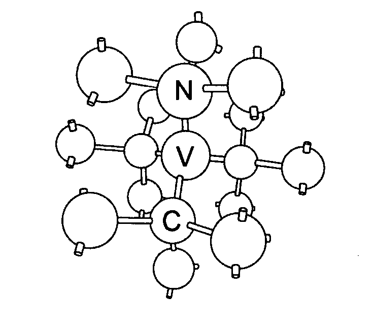
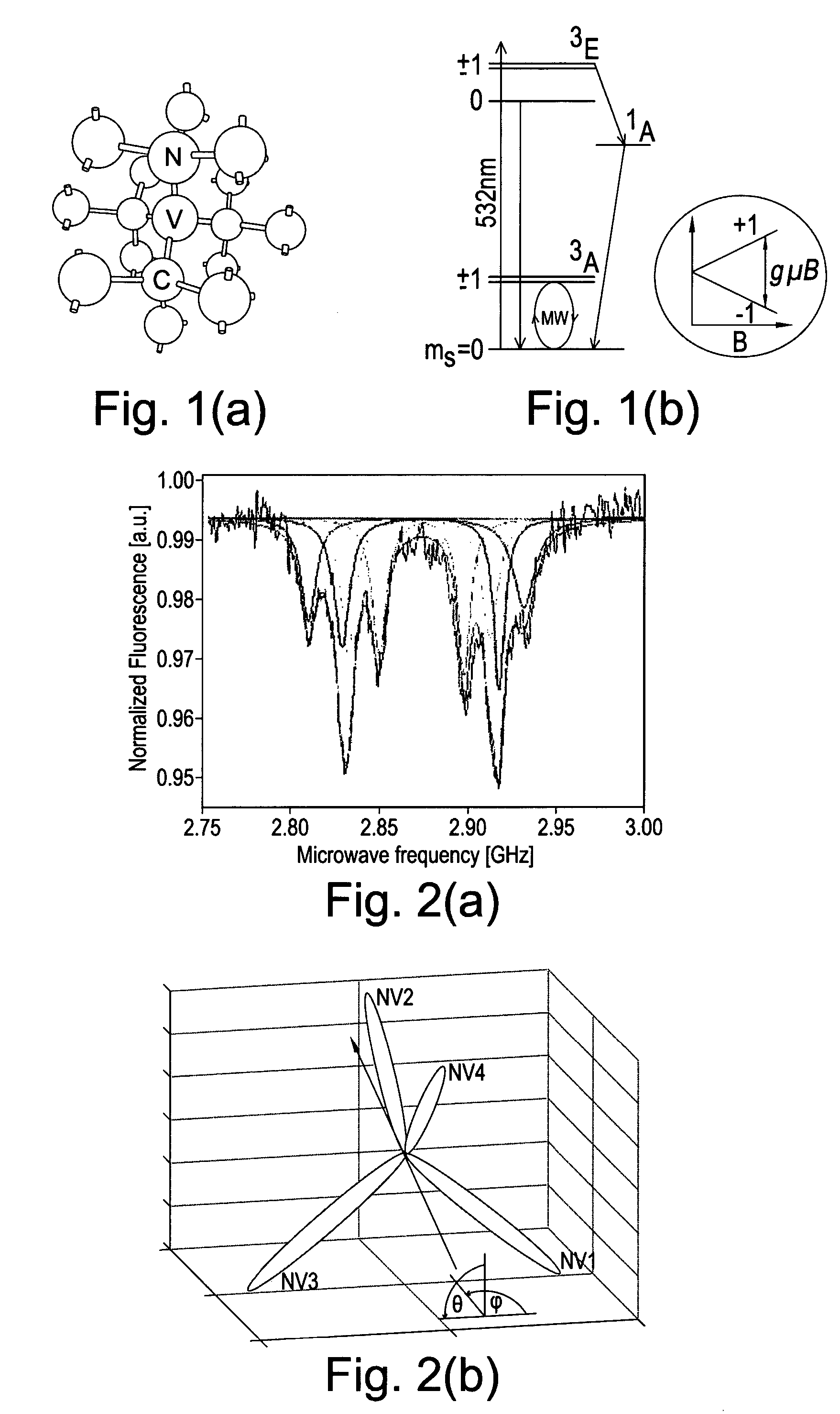
D2d
[0069]In a crystal with Td symmetry there are three possible symmetry related sites (orientations) of a defect with D2d symmetry. If all symmetry related sites are equally probably then the defect is randomly oriented.
[0070]If the probability of finding one particular site is n (where 0≦n≦1) and that for each of the other two (1−n) / 2 then the degree of preferential orientation can vary between completely preferentially oriented (n=1; 100% preferentially aligned), randomly oriented (n=⅓; 0% preferentially aligned) to oriented with equal probability in only two of the three possible symmetry related sites (n=0).
[0071]If the probabilities of occupancy of the three possible symmetry related sites are all different, say n, (1−n−p) / 2 and (1−n+p) / 2 then all possibilities for different distributions amongst the three symmetry related sites are bounded by the lines 0≦n≦1, p≧0 and n+p≦1.
example 2
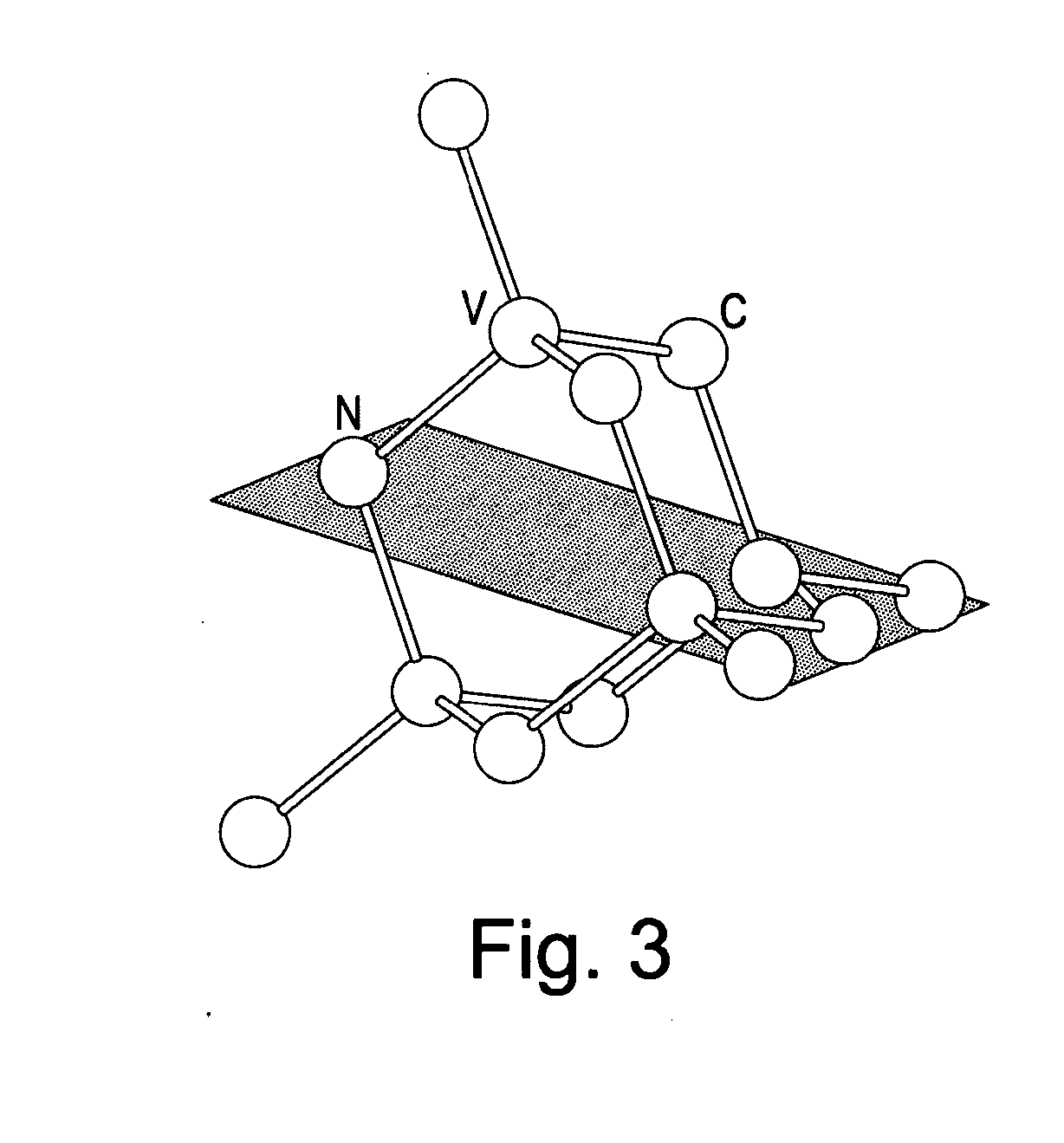
C3v
[0072]Four directions along which the trigonal axis of a symmetry related site can be oriented: [111], [ 111], [111] and [ 111] (and their inverses if the defect does not posses inversion symmetry) and labelled a, b, c, d
[0073]Consider growth direction along [001]:
[0074]The symmetry axes of the sites (a), (b), (c) and (d) make equal angles with respect to the growth direction (arccos(√{square root over (⅓)})). No preferential orientation (0% preferential alignment) of trigonal defects is expected for growth along the [001]. The same argument applies for growth along all (100) directions.
[0075]Consider growth direction along [110]:
[0076]The symmetry axes of the sites (a) and (b) make equal angles with respect to the growth direction (arccos(√{square root over (⅔)})). The symmetry axes of the sites (c) and (d) make equal angles with respect to the growth direction (90°).
[0077]Thus sites (a) and (b) can be treated as equivalent and sites (c) and (d) treated as equivalent.
[0078]If t...
synthesis example
[0141]A synthetic type Ib HPHT diamond plate with a pair of approximately parallel major faces within approximately 5° of (001) was selected. The plate was fabricated into a square substrate suitable for homoepitaxial synthesis of single crystal CVD diamond material by a process including the following steps:
i) laser cutting of the substrate to produce a plate with all edges;
ii) lapping and polishing the major surface upon which growth is to occur, the lapped and polished part having dimensions about 4.0 mm×4.0 mm by 300 μm thick, with all faces {100}. The defect level at or below the substrate surface is minimised by careful preparation of the substrate as disclosed in EP 1 292 726 and EP 1 290 251. It is possible to reveal the defect levels being introduced by this processing by using a revealing plasma etch. It is possible routinely to produce substrates in which the density of defects measurable after a revealing etch is dependent primarily on the material quality and is below ...
PUM
| Property | Measurement | Unit |
|---|---|---|
| Fraction | aaaaa | aaaaa |
| Fraction | aaaaa | aaaaa |
| Fraction | aaaaa | aaaaa |
Abstract
Description
Claims
Application Information