

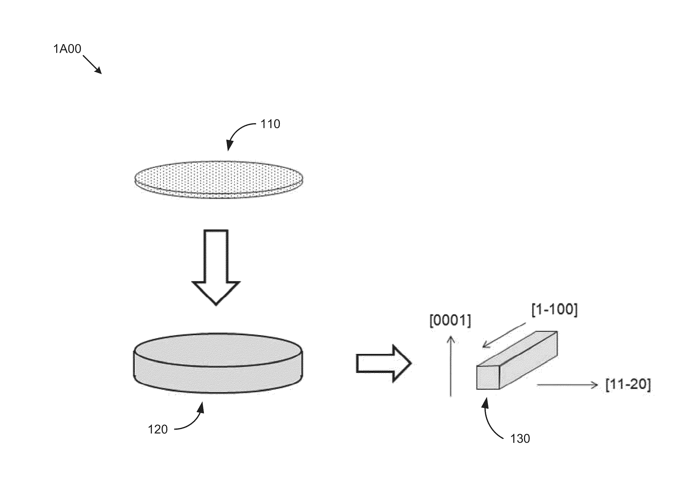
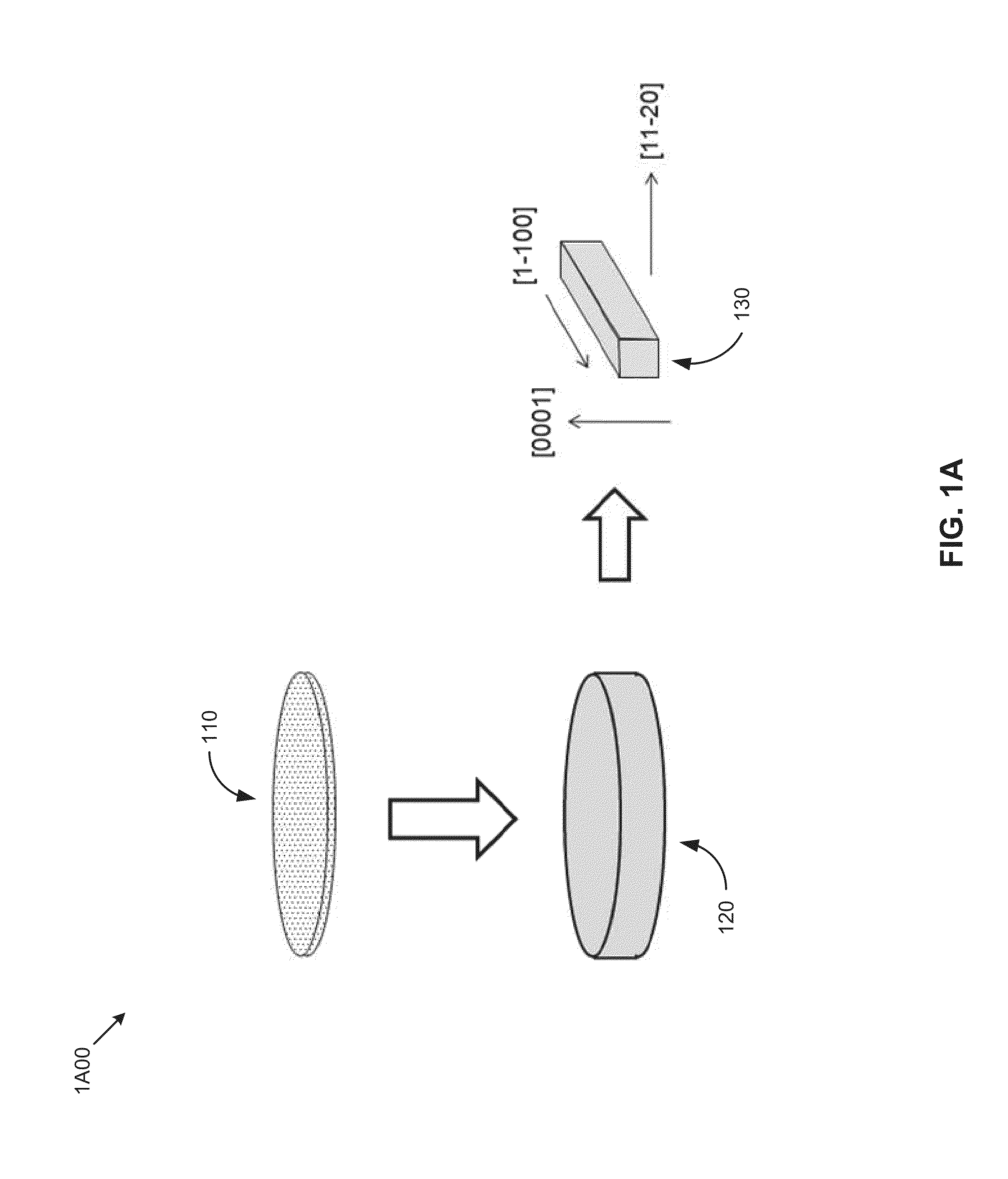
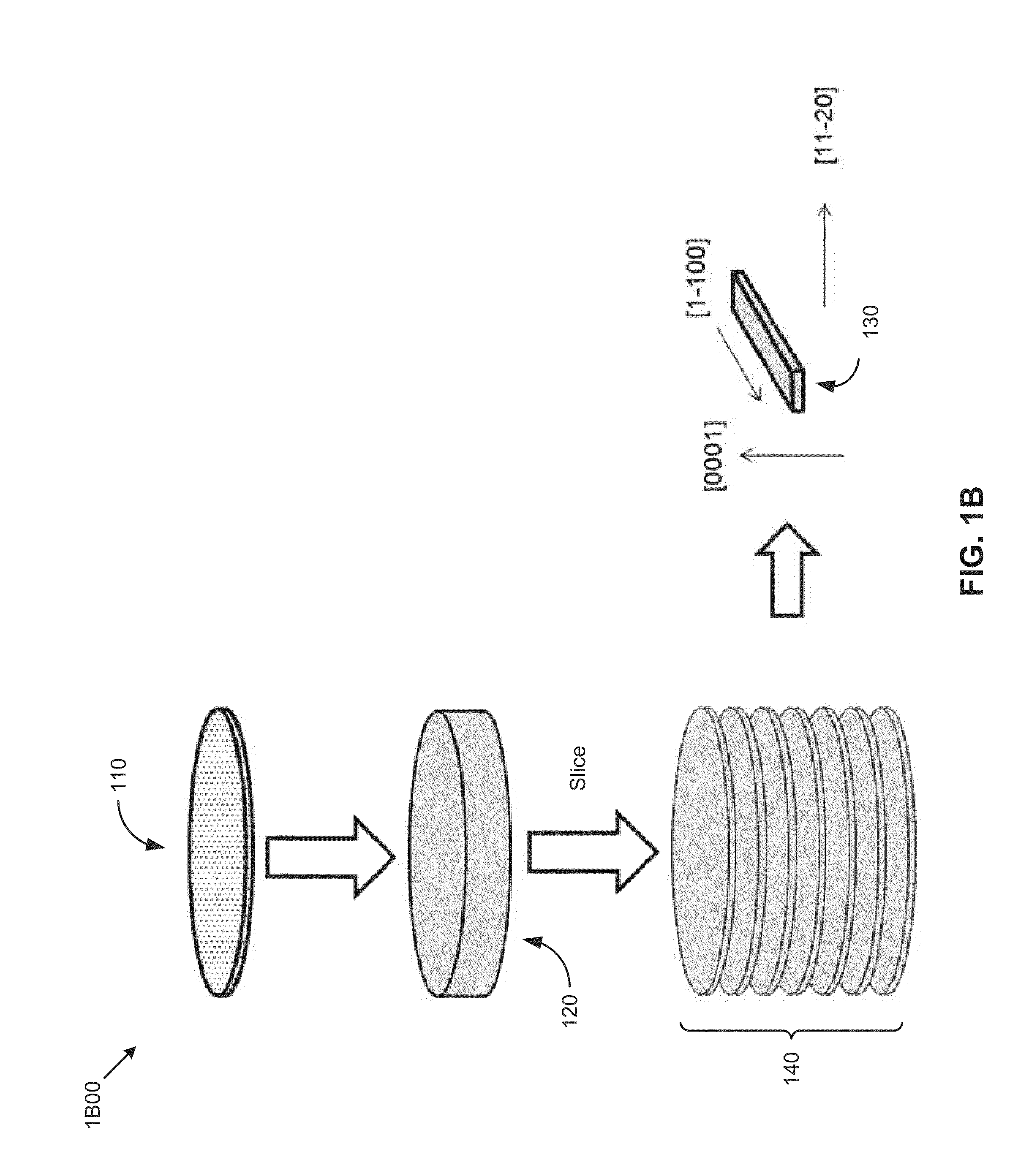
Large Area, Low-Defect Gallium-Containing Nitride Crystals, Method of Making, and Method of Use
a gallium-containing nitride and crystal technology, applied in the manufacture of final products, instruments, semiconductor lasers, etc., can solve the problems of additional defects, thermal expansion mismatch, impurities, tilt boundaries, and damage to epitaxially grown layers, and achieve the effect of reducing the number of defects, and reducing the quality of the devi
- Summary
- Abstract
- Description
- Claims
- Application Information
AI Technical Summary
Benefits of technology
Problems solved by technology
Method used
Image

Examples
example 1
[0145]A c-plane oriented bulk GaN crystal grown by HVPE, approximately 0.3 millimeters thick, was provided for use as a seed crystal for ammonothermal growth. The seed crystal was placed inside a silver capsule along with a 33%-open-area baffle, approximately 41.8 grams of polycrystalline GaN nutrient, 2.6 grams of NH4F mineralizer, and 30.0 grams of ammonia and the capsule was sealed. The capsule was placed in an internally-heated high pressure apparatus and heated to temperatures of approximately 647 degrees Celsius for the upper, nutrient zone and approximately 665 degrees Celsius for the lower, crystal growth zone, maintained at these temperatures for approximately 45 hours, and then cooled and removed. The crystal, which grew to a thickness of approximately 1.6 millimeters, was then examined under a microscope. The crystal was then etched in conditioned H3PO4 in a beaker, stirred at 130 revolutions per minute, at a hot plate temperature of approximately 350 degrees Celsius for ...
example 2
[0146]An m-plane oriented bulk GaN crystal grown by HVPE, approximately 0.3 millimeters thick, was provided for use as a seed crystal for ammonothermal growth. The seed crystal was placed inside a silver capsule along with a 33%-open-area baffle, approximately 49.0 grams of polycrystalline GaN nutrient, 2.6 grams of NH4F mineralizer, and 29.2 grams of ammonia and the capsule was sealed. The capsule was placed in an internally-heated high pressure apparatus and heated to temperatures of approximately 645 degrees Celsius for the upper, nutrient zone and approximately 665 degrees Celsius for the lower, crystal growth zone, maintained at these temperatures for approximately 45 hours, and then cooled and removed. The crystal, which grew to a thickness of approximately 1.4 millimeters, was then lapped at an angle of approximately 3.7 degrees to allow for examination of the GaN material properties as a function of thickness above the interface with the HVPE seed crystal, and the freshly pr...
example 3
[0149]An m-plane oriented bulk GaN crystal grown by HVPE, approximately 0.3 millimeters thick, was provided for use as a seed crystal for ammonothermal growth. The seed crystal was placed inside a silver capsule along with a 33%-open-area baffle, approximately 35.9 grams of polycrystalline GaN nutrient, 2.6 grams of NH4F mineralizer, and 30.4 grams of ammonia and the capsule was sealed. The capsule was placed in an internally-heated high pressure apparatus and heated to temperatures of approximately 645 degrees Celsius for the upper, nutrient zone and approximately 665 degrees Celsius for the lower, crystal growth zone, maintained at these temperatures for approximately 40 hours, and then cooled and removed. The crystal grew to a thickness of approximately 0.8 millimeters. The crystal was then etched in conditioned H3PO4 in a beaker, stirred at 130 revolutions per minute, at a hot plate temperature of approximately 350 degrees Celsius for 60 minutes. The conditioned H3PO4 was prepar...
PUM
| Property | Measurement | Unit |
|---|---|---|
| Temperature | aaaaa | aaaaa |
| Temperature | aaaaa | aaaaa |
| Length | aaaaa | aaaaa |
Abstract
Description
Claims
Application Information