Process for forming a crack in a material
a technology of cracks and materials, applied in the direction of basic electric elements, semiconductor/solid-state device manufacturing, electric devices, etc., can solve the problems of complex mechanisms of he—h co-implantation, high implantation parameter sensitive techniques, and complicating the use of this techniqu
- Summary
- Abstract
- Description
- Claims
- Application Information
AI Technical Summary
Benefits of technology
Problems solved by technology
Method used
Image
Examples
example 1
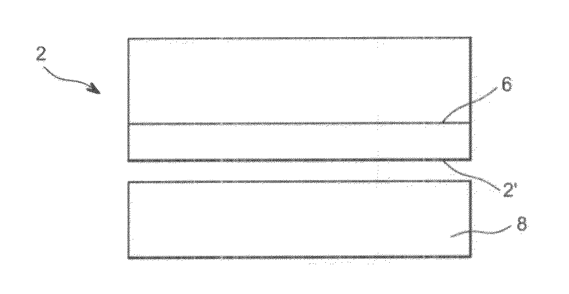
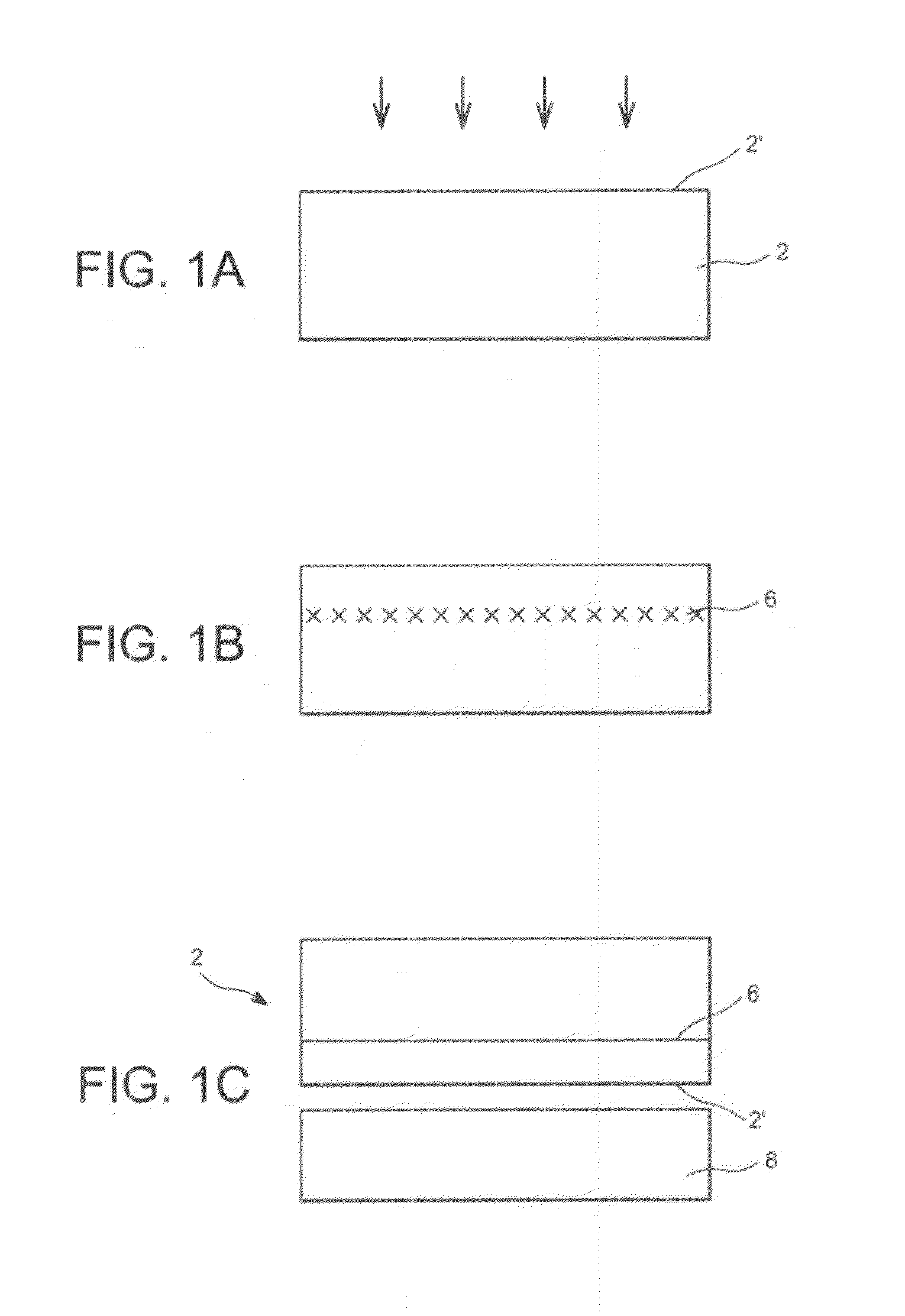
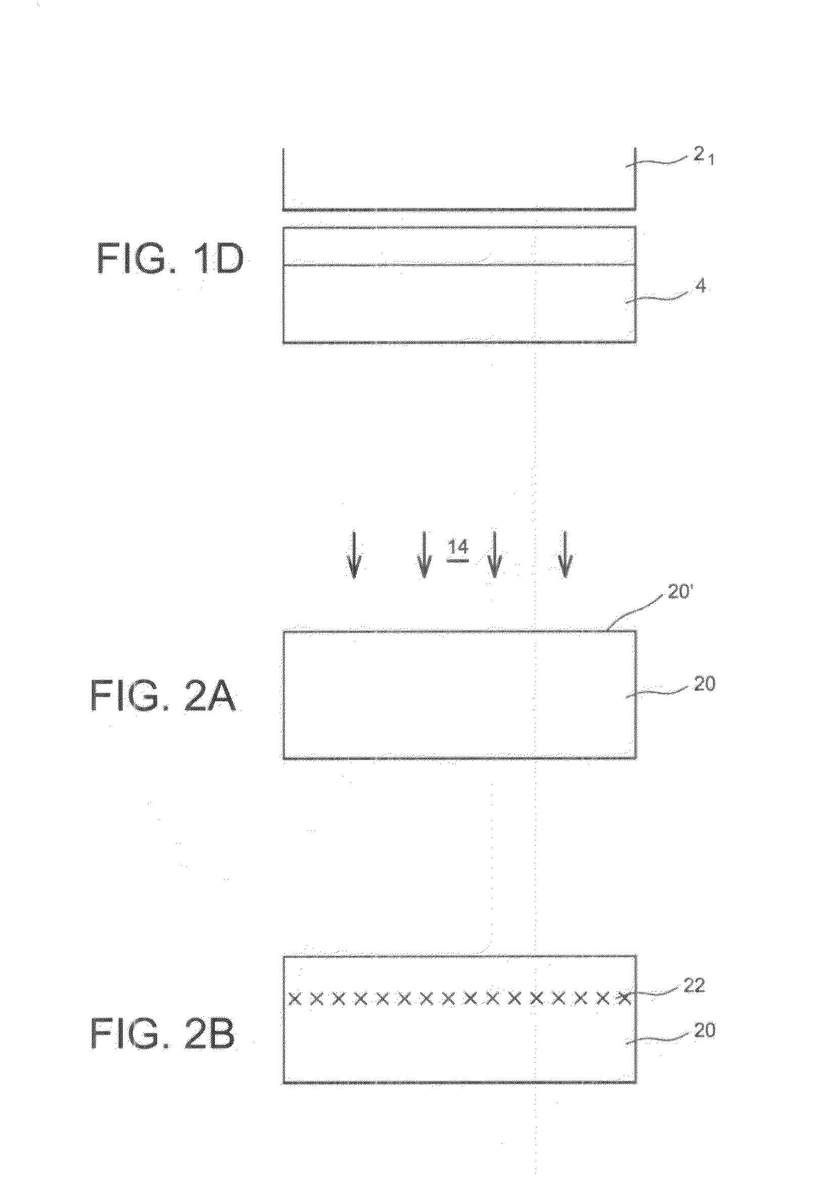
[0077]A substrate 20 made of Silicon (100) is provided with a 100 nm thick layer of thermal oxide SiO2.
[0078]It is implanted under the following conditions, the steps being those in FIGS. 2A-2F:
[0079]a first lithium implantation is performed, at an energy of 210 keV and with a dose of 1015 / cm2,
[0080]a second hydrogen implantation is then performed, at an energy of 100 keV and with a dose of 4.5×10¹⁶ / cm2.
[0081]The implanted substrate is then bonded onto a sapphire substrate 19 by means of direct or molecular bonding or assembly (FIG. 2E).
[0082]A Si / Sapphire heterostructure is obtained after bonding. As the thermal expansion coefficients (TEC) of Si and sapphire are very different (TEC Si=2.31.10−6 / K and TEC sapphire=6.35.10−6 / K), the Si / sapphire bond cannot be heated to a temperature greater than ˜350° C.: above this temperature, systematic detachment of the structures is observed.
[0083]The fracture formation treatment then consists for example of annealing at 250° C. for 1 hour.
[008...
example 2
[0086]A P-type Si substrate (111) undergoes lithium introduction by means of diffusion, under the following conditions:
[0087]a layer of Li is firstly deposited on the Si surface by means of vacuum evaporation (at 2.10−6 Torr), at ambient temperature,
[0088]the Li is then diffused in the Si, by means of vacuum annealing (1.10−6 Torr), at 800° C. for 10 min.
[0089]The excess Li on the surface of the Si substrate is removed by rinsing the wafer in methanol.
[0090]This gives a typical diffusion profile, similar to that shown in FIG. 4A, taken from the article by A. Keffous et al. cited above, but with higher Li concentration levels (in this figure, the * symbols correspond to experimental values, with a diffusion temperature of 425° C. and a diffusion time of 4 min; the black circular dots correspond to PCID simulation results, under the same conditions). Indeed, the Li concentration on the surface of the substrate (or at a zero depth in FIG. 4A) corresponds to the solubility of Li in Si, ...
PUM
 Abstract
Description
Claims
Application Information
 - R&D
- Intellectual Property
- Life Sciences
- Materials
- Tech Scout
- Unparalleled Data Quality
- Higher Quality Content
- 60% Fewer Hallucinations
Browse by: Latest US Patents, China's latest patents, Technical Efficacy Thesaurus, Application Domain, Technology Topic, Popular Technical Reports.
© 2025 PatSnap. All rights reserved.Legal|Privacy policy|Modern Slavery Act Transparency Statement|Sitemap|About US| Contact US: help@patsnap.com


