Flat sic semiconductor substrate

a technology of silicon carbide and semiconductor substrate, which is applied in the direction of manufacturing tools, polycrystalline material growth, after-treatment details, etc., to achieve good global and local flatness and thickness performan

Active Publication Date: 2014-05-01
SK SILTRON CSS LLC
View PDF4 Cites 342 Cited by
  • Summary
  • Abstract
  • Description
  • Claims
  • Application Information

AI Technical Summary

Benefits of technology

[0020]Various embodiments provide methods for efficiently polishing an SiC wafer to achieve a surface free of mechanical damage and applying an epitaxial layer, and simultaneously delivering superior performance with respect to flatness. Without being bound by any theory, some disclosed methods are predicated on the discovery that the propagation of polishing damage from abrasives used on SiC follows a unique behavior. Strategic integration of SiC wafer polishing methods involving different abrasives, intermediate process targets and batch processing equipment with larger diameter lap / polish tables have been found to result in a cost efficient process meeting the process duration and quality goals suitable to sell the product within the power semiconductor industry.
[0023]According to other aspects, a polished SiC wafer having a back surface and a front surface conditioned for epitaxial deposition is provided, wherein the front surface has rms roughness of Rq<15 Å. Due to the nature of the double side polishing process, the back surface has similar value of RMS roughness. Further, the wafer has total thickness variation (TTV) of 0.1-5 μm and local thickness variation (LW) of 0.1-1.5 μm, based on a one square centimeter site size. Additionally, the wafer exhibits warp between 0.1 and 35 μm and site front side least squares focal plane range of 0.01-0.3 μm, based on a one square cm site size. When the polished wafer is used for epitaxial deposition of SiC layer on the front surface thereof, the wafer retains good global and local flatness and thickness performance.

Problems solved by technology

U.S. Pat. No. 8,436,366 does not disclose a process which will establish low values of global and local thickness variations and flatness on either polished wafers or polished wafers with epitaxial layers.

Method used


Image

  • Flat sic semiconductor substrate
  • Flat sic semiconductor substrate

Examples


example 1

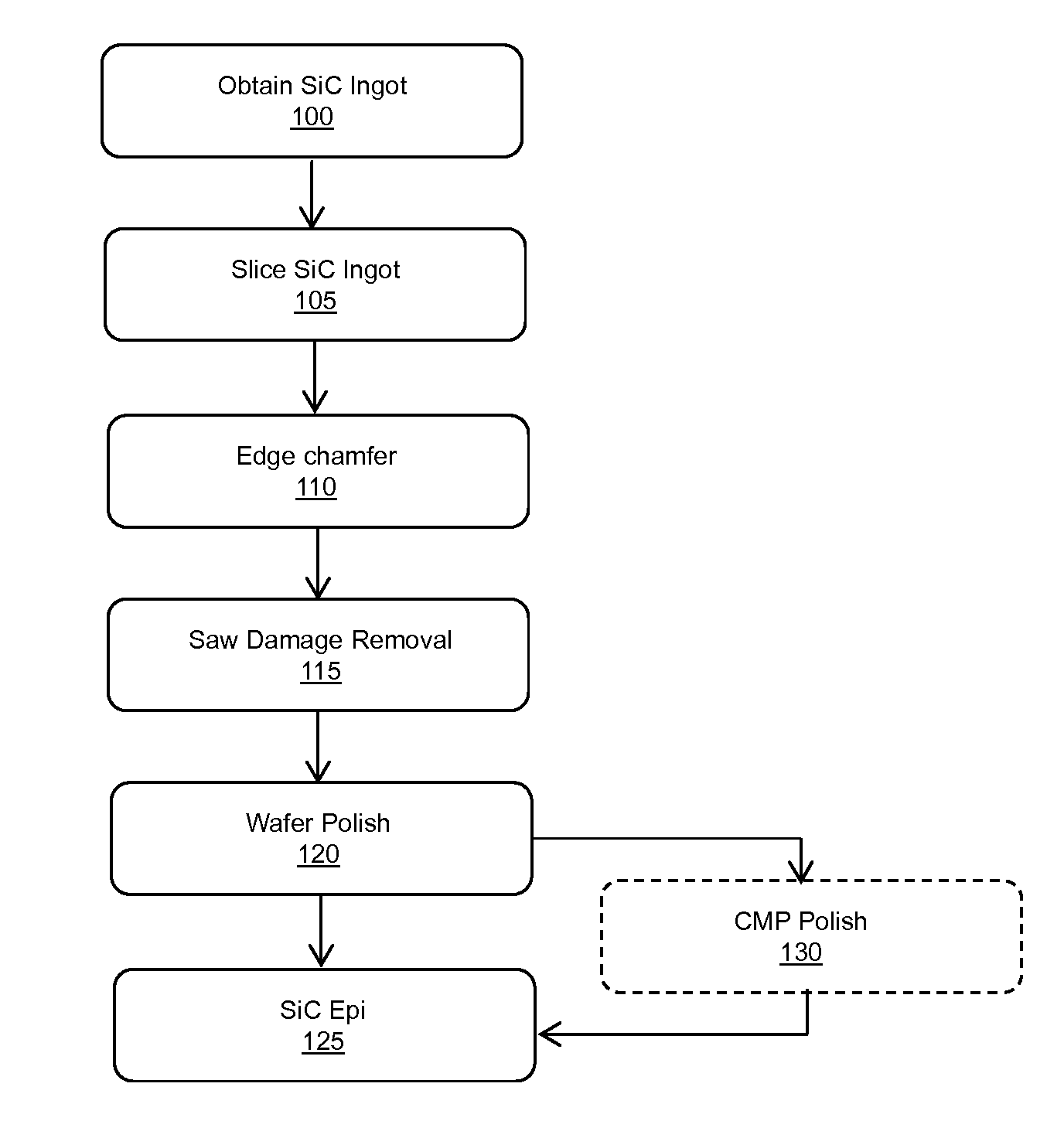
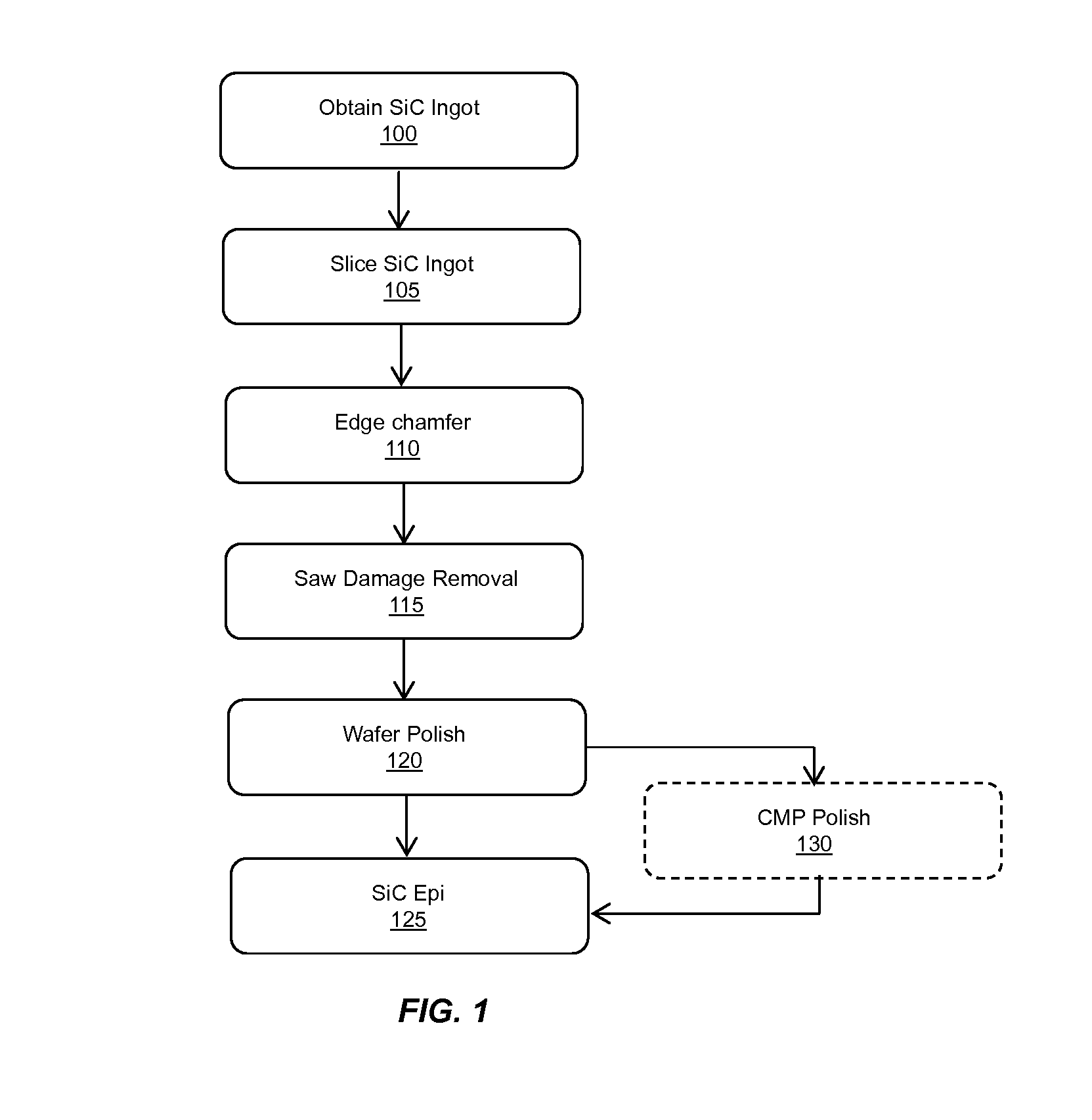
[0072]The process flow disclosed above and illustrated in FIG. 1, was employed to fabricated 4H—SiC wafers of 75 mm and 100 mm diameters. The wafers exhibited resistivity range of 0.015-0.028 ohm cm. For steps 100-105-110, SiC ingots were machined into right cylinders. The cylindrical ingots were mounted on a plastic beam and placed into a multiwire saw. The ingots were cut using wire and a flow of diamond slurry directed onto the periphery of the ingot. The beam was removed from the saw and based into a bath to separate the slices from the beam. The slices were rinsed and placed into a cassette. The wafers were transferred to an automated edge grinding system where a trapezoidal edge profile was formed using a diamond wheel. The process follows the guidelines of SEMI Standard M55.

[0073]For step 115, saw damage removal was conducted using lapping or grinding, as indicated. Lapping was performed simultaneously on both wafer sides using lapping machine with diameter >40 inches. Wafers...


PUM

PropertyMeasurementUnit
thicknessaaaaaaaaaa
thicknessaaaaaaaaaa
total thickness variationaaaaaaaaaa

Abstract

Methods for manufacturing silicon carbide wafers having superior specifications for bow, warp, total thickness variation (TTV), local thickness variation (LTV), and site front side least squares focal plane range (SFQR). The resulting SiC wafer has a mirror-like surface that is fit for epitaxial deposition of SiC. The specifications for bow, warp, total thickness variation (TTV), local thickness variation (LTV), and site front side least squares focal plane range (SFQR) of the wafer are preserved following the addition of the epitaxy layer.

Description

CROSS-REFERENCE TO RELATED APPLICATIONS[0001]This application claims the benefit of, and priority to, U.S. Provisional Patent Application No. 61 / 719,310, filed on Oct. 26, 2012, entitled “FLAT SIC SEMICONDUCTOR SUBSTRATE,” the entire disclosure of which is hereby incorporated herein by reference.BACKGROUND[0002]1. Field[0003]This disclosure relates to fabrication of semiconductor wafers and, more specifically, to semiconductor wafers made of silicon carbide.[0004]2. Related Arts[0005]The semiconductor chip industry owes much of its success to the natural properties of silicon. These properties include the ease of growing native oxide (SiO2), the excellent insulating properties of its native oxide, and the relative ease of fabrication of silicon wafers and devices within the silicon wafers. For example, silicon and its native oxide are easily etched using either wet or dry plasma etch processes. Consequently, many processes have been developed for fabrication of highly pure (99.99999...

Claims


Application Information

Patent Timeline
Patent Type & Authority Applications(United States)
IPC IPC(8): H01L29/30H01L21/306
CPCH01L29/30H01L21/30625B24B1/00B24B7/228B24B9/065B24B37/28C30B29/36C30B33/00H01L21/02008H01L21/02013H01L21/02024H01L21/0243H01L21/02378H01L21/02658H01L21/02529H01L29/1608H01L21/02019H01L21/02021H01L21/02035
Inventor LOBODA, MARKPARFENIUK, CHRISTOPHER
Owner SK SILTRON CSS LLC
Why Eureka
Try Eureka