

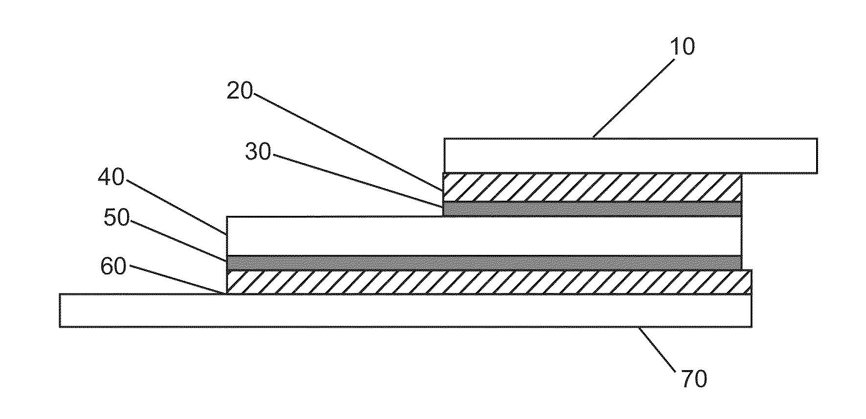
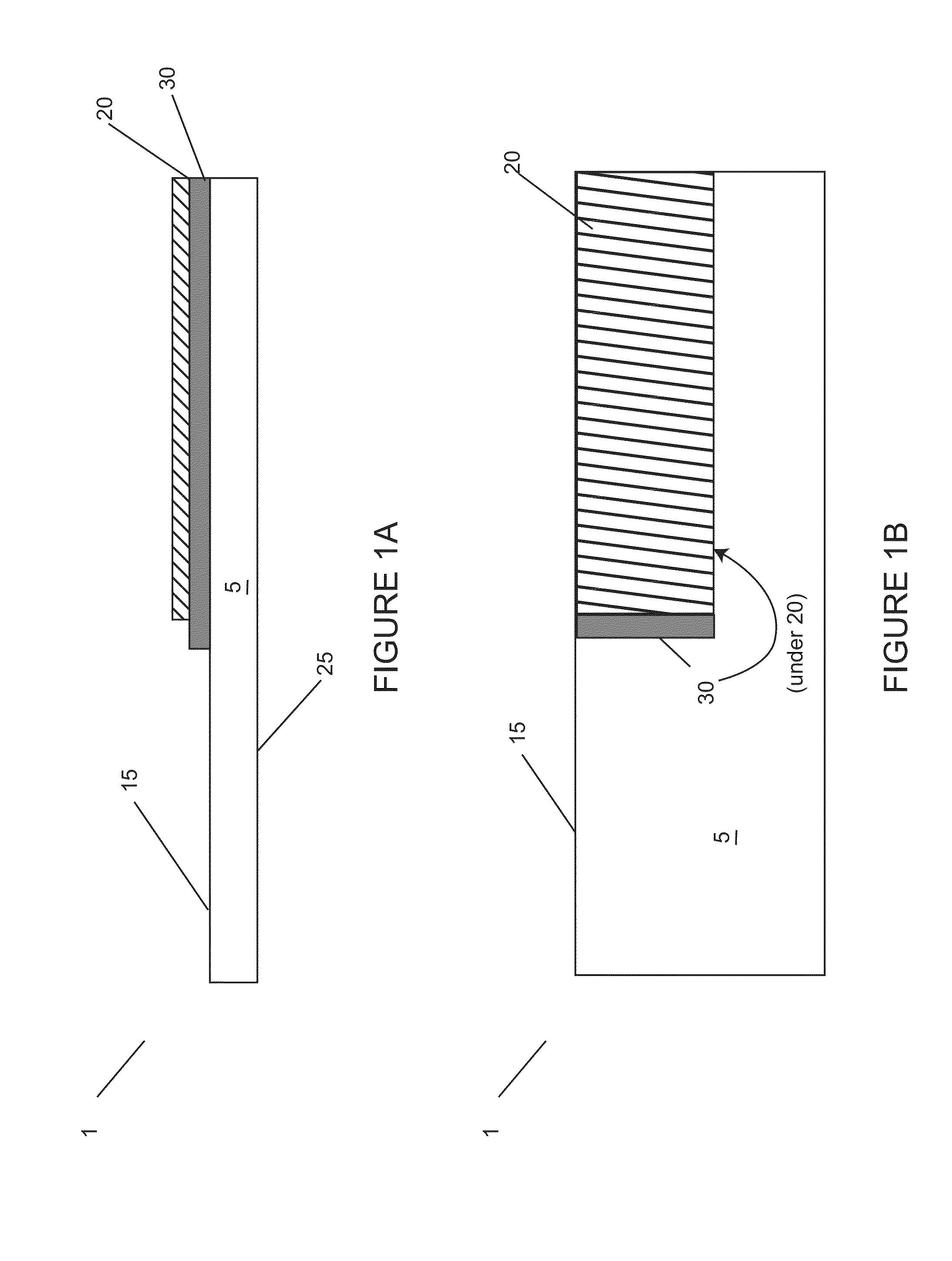
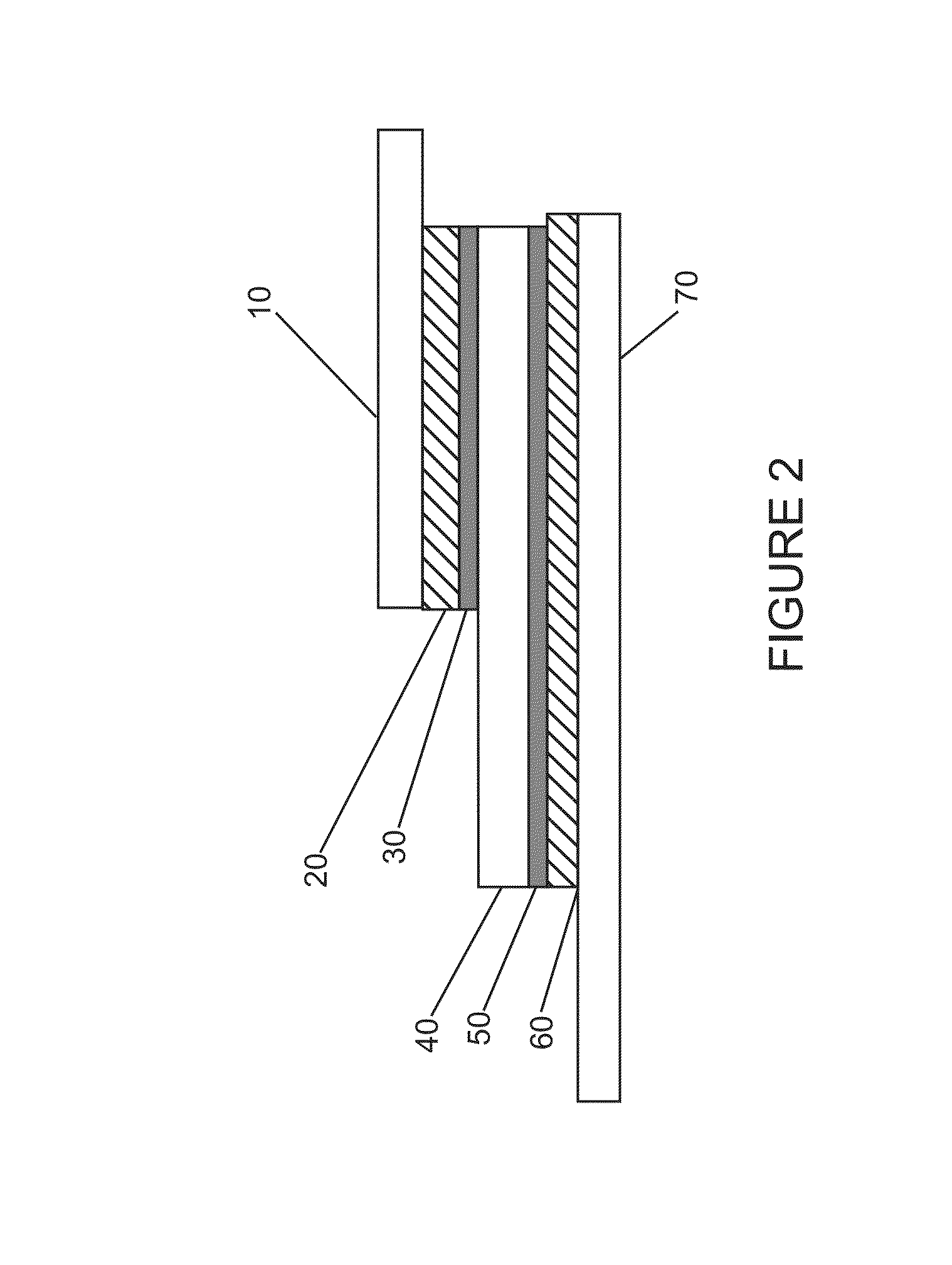
Semiconductor packaging containing sintering die-attach material
a technology of die-attaching materials and semiconductors, applied in the direction of semiconductor/solid-state device details, semiconductor devices, electrical equipment, etc., can solve the problems of current film, low thermal conductivity of film-based die-attach materials, and low thermal conductivity of wbc-based die-attach materials
- Summary
- Abstract
- Description
- Claims
- Application Information
AI Technical Summary
Benefits of technology
Problems solved by technology
Method used
Image

Examples
example 1
[0097]Four sintering films were prepared for application to a wafer. The films contained 8 micron (average) spherical copper powder, Sn80:Bu20 alloy powder supplied in the configurations indicated below in Table 1, and a fluxing binder (16 weight % glutaric acid, 84 weight % N,N,N′,N′ tetrakis(2-hydroxyethyl) ethylenediamine). The films were cast from a solvent-based varnish (9 parts fluxing binder, 30 parts cyclopentantone, 41 parts copper, and 50 parts alloy), onto a polymer carrier (polyethyleneterephthalate), dried at 90 C.° to evaporate the solvent and applied to a wafer by lamination in a heated vacuum frame with 25° C. to 100° C. ramp in temperature at 5° C. / min. The wafers were then singulated by dicing into individual die with a wafer saw equipped with a diamond blade. The die were placed onto silver-plated copper lead frames and sintered in a nitrogen environment in a box oven at 260° C. for 90 minutes. Upon cooling, the sintered die-lead frame assemblies were sheared at 2...
example 2
[0100]Four sinterable films were prepared for application to wafers. The films contained 8 micron (average) spherical copper powder, Sn80:Bu20 alloy particles supplied in particle size ranges, shapes and average surface areas indicated below in Table 2, and the fluxing binder indicated in EXAMPLE 1. The films were cast from a solvent-based varnish onto a polymer carrier, dried to evaporate the solvent and strips of the film were applied to glass slides by lamination as described in EXAMPLE 1. The strips of film on glass slides were then sintered as described above in EXAMPLE 1 as described above, and the electrical resistance was measured using an ohmmeter in a four-point-probe configuration. The electrical resistivity was calculated based on the measured resistance and dimensions of the strips
(resistance*width*thickness / length (all dimensions in cm).
[0101]The results, which are summarized in Table 2, indicate that both the alloy particle size distribution and average surface area w...
example 3
[0103]A sinterable die-attach paste was prepared containing 91 weight percent metal particles and the Organics Mixture detailed below in Table 3. Briefly, the metals were weighed into Hobart bowl and blended. The organic components were weighed into separate bowl, the metals were then added to the organic components and hand mixed to wet the metals. The combination containing the components listed in Table 4 was mixed in Hobart mixer for 5 min, and then transferred to 1.5 L D.P. mixing pot, and mix with degassing for 20 min. at 30 rpm, in a 25° C. waterbath. The final mixture was filtered through a 100-150-100 disc filter prior to use.
TABLE 3Organic MixtureIngredientWeight %R1001 - Ester oligomer25.00Hypox RF 134112.50DABA / TEOA33.33A3008 - Antifoam 14004.17S4001 - Butyl Carbitol25.00100.00
TABLE 4Final MixIngredientWeight %Organics Mix w / BC pre-added11.65F2024 - 2 um Mitsui Copper14.56F2014 - 8 um Cu Powder, HK-50038.84F2022 - 80Sn / 20Bi, type 6, HK-50034.95100.00
[0104]The paste mixtu...
PUM
 Abstract
Description
Claims
Application Information